

Wideband CMOS gain stage
a gain stage and wideband technology, applied in the field of amplifiers, can solve problems such as gate oxide breakdown and/or draining to bulk junction punching through
- Summary
- Abstract
- Description
- Claims
- Application Information
AI Technical Summary
Benefits of technology
Problems solved by technology
Method used
Image

Examples
Embodiment Construction
Table of Contents
I. Bipolar Gain Stage
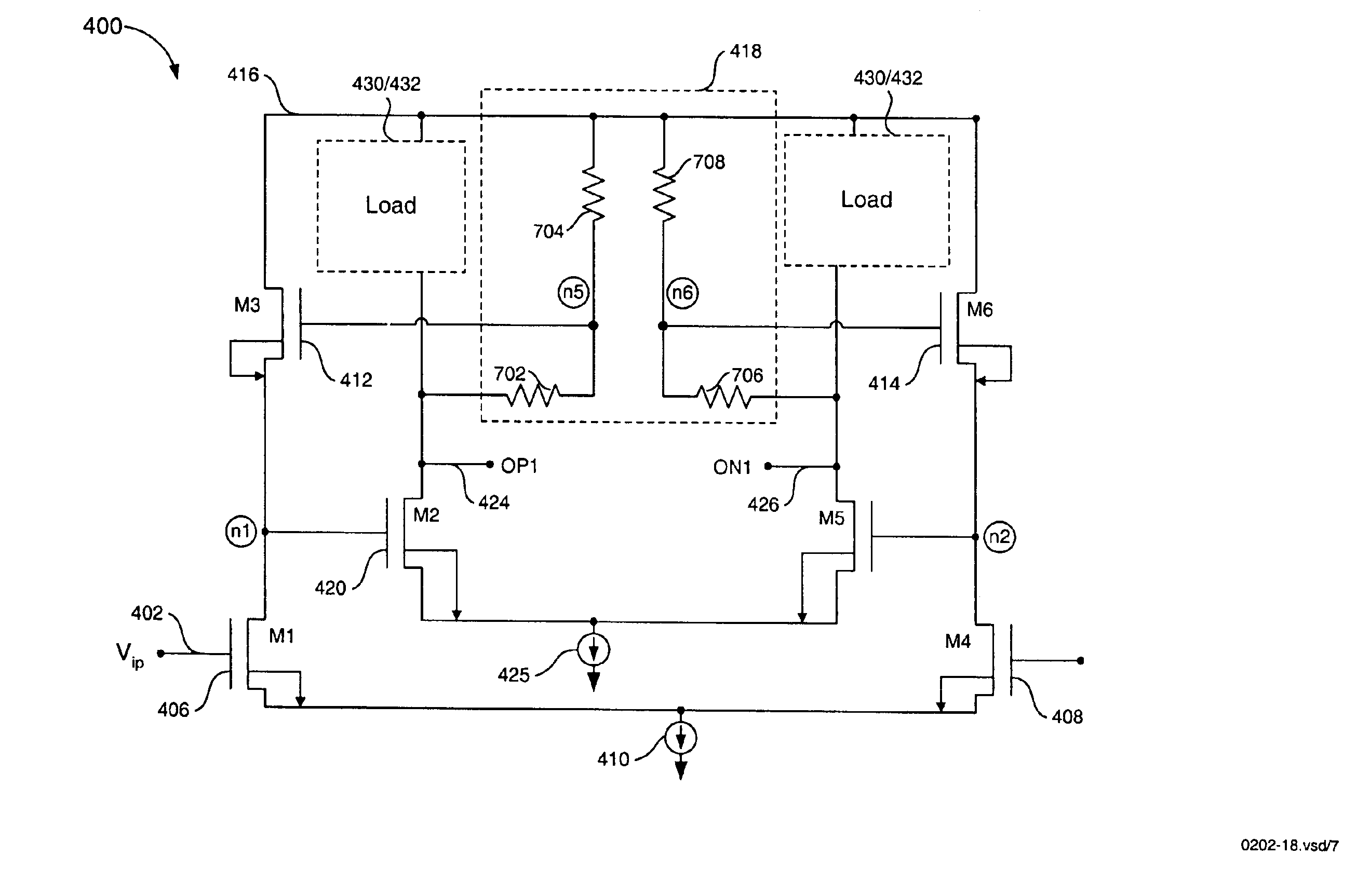
II. CMOS Gain Stage
[0022]A. Introduction[0023]B. Bias Network Configured for an Output Source Follower[0024]C. Bias Network Configured for Omission of an Output Source Follower[0025]D. Supply Voltage and Drain-to-Bulk Junction Punch-Through[0026]E. PVT Independent Gain[0027]F. Bandwidth Enhancement
III. Conclusions
I. Bipolar Gain Stage
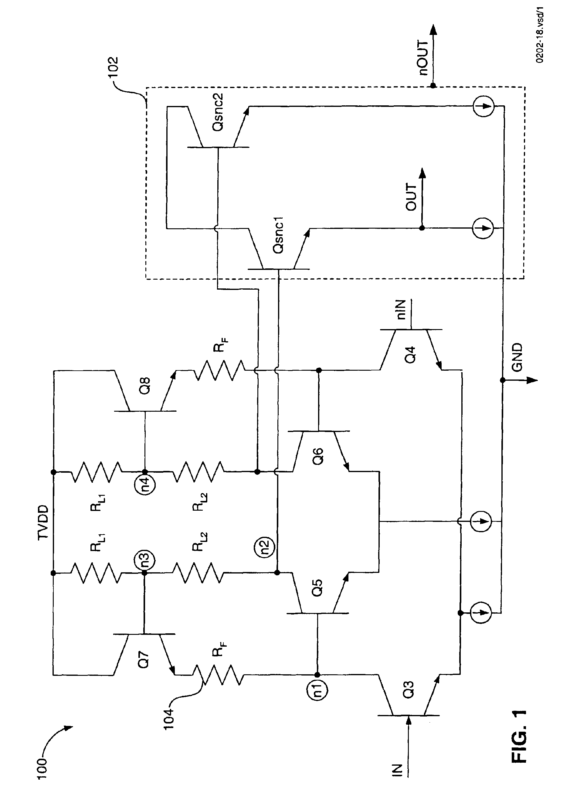
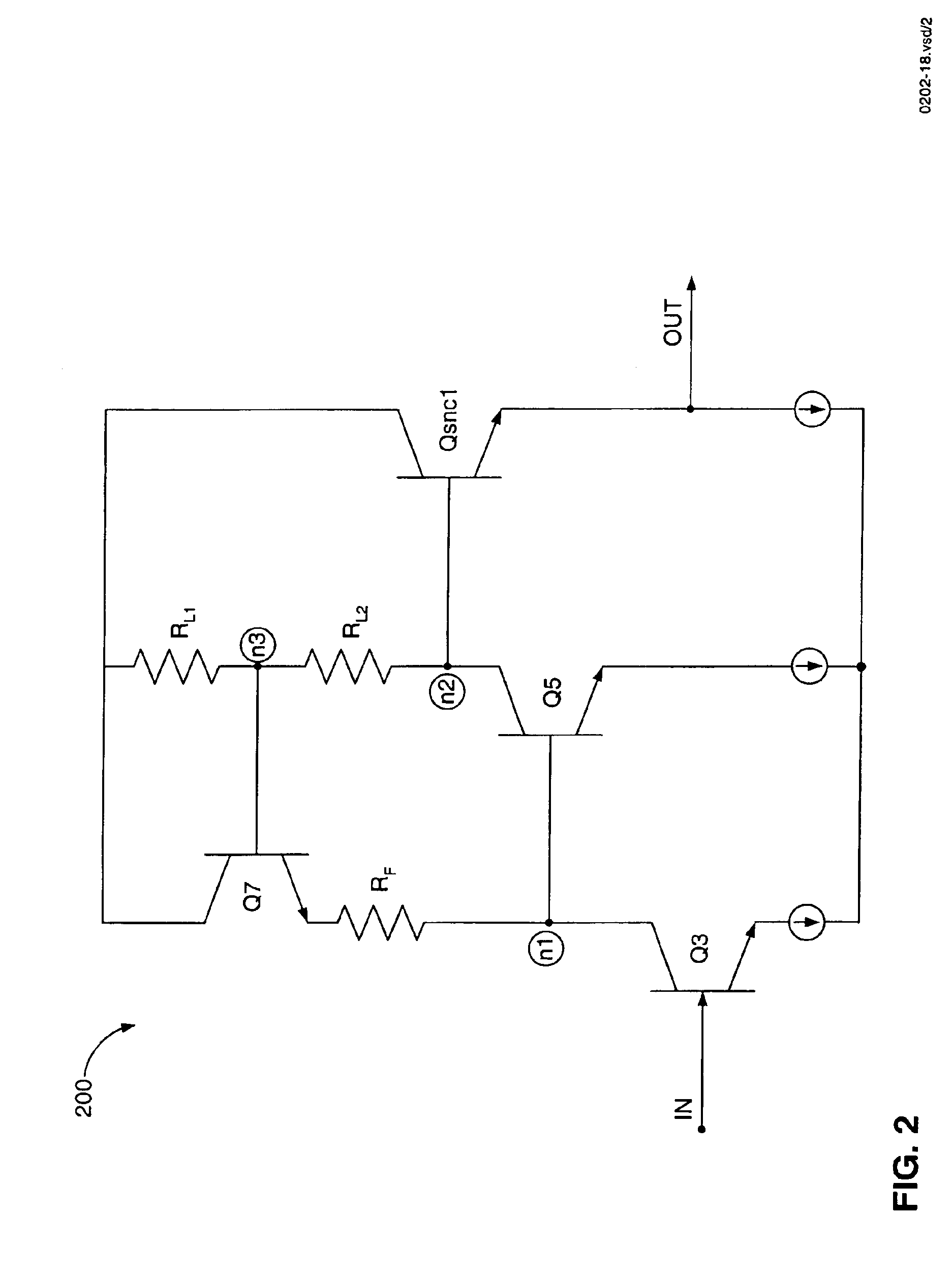
[0028]FIG. 1 is a schematic diagram of a bipolar amplifier 100. FIG. 2 is a schematic diagram of a bipolar “hay circuit”200, which is taken from the bipolar amplifier 100 in FIG. 1. A gain of the bipolar amplifier 100 can be determined by analyzing the hay circuit 200.
[0029]The hay circuit 200 includes bipolar transistors Q3, Q5, and Q7, and resistors RL1 and RL2. The gain of the hay circuit 200 and of the bipolar-implemented amplifier 100 can be determined by denoting a resistive divider ratio “x,” as shown in equation 1: x=RL 1(RL 1+RL 2)EQ. (1)
[0030]Transconductances of the transistors Q3, Q5, Q7 are denot...
PUM
 Abstract
Description
Claims
Application Information