Dielectric waveguide type filter and branching filter

a dielectric waveguide and filter technology, applied in the direction of waveguides, electrical devices, coupling devices, etc., can solve the problems of reducing the diameter, easy to be caused between the conductive vias, and the abovementioned structure of the waveguide filter, and achieves easy manufacturing, high productivity, and small size.

Inactive Publication Date: 2005-08-09
KYOCERA CORP
View PDF11 Cites 31 Cited by
  • Summary
  • Abstract
  • Description
  • Claims
  • Application Information

AI Technical Summary

Benefits of technology

[0020]According to the dielectric waveguide type filter of the present invention, the resonator is constituted by a dielectric having a higher dielectric constant than that of the dielectric forming the dielectric waveguide. Regardless of a signal frequency, the resonator can be formed with a constant width of dielectric waveguide, and the resonator and the filter can be easily designed. Further, the conductive vias constituting side walls of the dielectric waveguide can be formed with a constant pitch, so that the dielectric waveguide type filter can be easily designed and manufactured. Further, according to the conventional method of manufacturing a multi-layered wiring substrate, the resonator and the filter can be easily contained in various kinds of multi-layered substrates. Furthermore, the dielectric waveguide filer can be easily manufactured by a sheet laminating method such as a green sheet laminating method, and therefore, it can be manufactured with high reliability and productivity and at low cost.
[0031]Further, it is preferable that the property of the abovementioned dielectric waveguide type filter can be easily controlled by providing a plurality of shortcut conductors and / or dielectric vias having another dielectric constant than that of the dielectric substrate for electrically connecting the main conductive layers to each other in the region enclosed by the main conductive layers and the conductive via groups.

Problems solved by technology

Such a waveguide filter having the abovementioned structure is very hard to manufacture since waveguide walls thereof are all formed of metal plates.
First, at the time of manufacturing, reducing the diameter and the pitch of the conductive vias 38 is limited. For example, when the via diameter is φ0.2 mm, it is preferable to make the via pitch 0.5 mm or more. This is because, if the via pitch becomes too small, cracks are apt to be caused between the conductive vias and the reliability is lessened.
Secondly, since the conductive vias 38 constitute E surface of the dielectric waveguide, the distance therebetween must be set to be less than ½ of the signal frequency in principle. When a low frequency is used, that is, when the signal wavelength is long, the size of the resonator 39 is large as shown in FIG. 13A, and therefore, the resonator 39 can be formed by sufficient number of conductive vias even with a via pitch of 0.5 mm or more. However, when a high frequency is used, the resonator 39 becomes short as shown in FIG. 13B, and therefore, only small number of conductive vias can be disposed on the sides enclosing the resonator 39. As the case may be, the conductive vias 38 cannot be arranged within the abovementioned limitation of the via pitch. Further, a dielectric waveguide having such conductive vias 38 is very hard to design, because the equivalent waveguide size changes with the via pitch.
However, it has a problem that works of its manufacturing, such as fitting of the waveguide filters 52, 53 to the waveguide filter 51, are difficult.
Consequently, it has a problem that the productivity is low and therefore the cost becomes high.
Further, since the size of the rectangular waveguide itself is large, a branching filter using the same becomes large and is hard to be small-sized in order to be used for movable body communication, inter-vehicle radars and the like.
However, it is difficult to manufacture dielectric blocks with precision.
Furthermore, since the strength of dielectric blocks is lower than that of the metal waveguide, cracks, breakage and the like are apt to be caused near the iris channels.
Therefore, dielectric blocks have low stability and have to be protected by other members when used.

Method used


Image

  • Dielectric waveguide type filter and branching filter
  • Dielectric waveguide type filter and branching filter
  • Dielectric waveguide type filter and branching filter

Examples


example 1

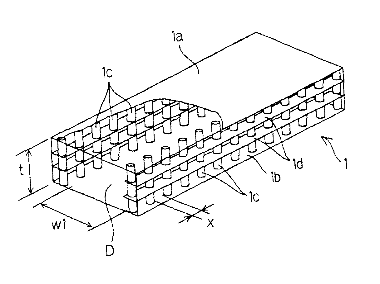
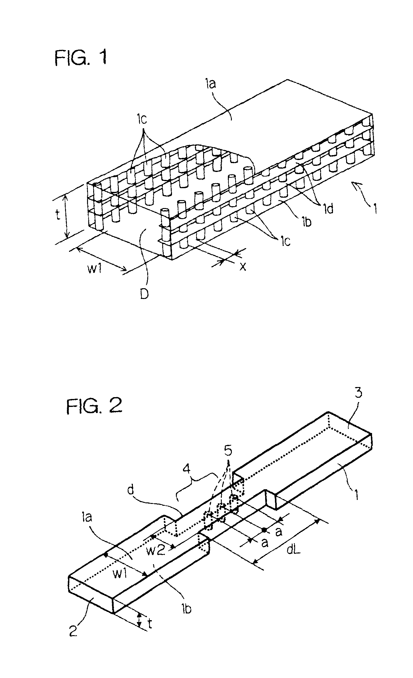
[0091]A dielectric waveguide type filter shown in FIG. 2 was manufactured. The transmittance characteristic of the filter is shown in FIG. 5. Parameters of the filter were as follows. Of the basic dielectric waveguide, the dielectric constant ∈r=4.9, the width of the waveguide W1=1.6 mm, and the thickness of the waveguide t=0.48 mm. Of the resonator 4, the width of the cutoff waveguide w2=0.8 mm, the length of the cutoff waveguide path dL=2.6 mm, the dielectric constant of the dielectric in the dielectric vias ∈d=20.0, the dielectric via diameter b=φ0.2 mm, and the dielectric via pitch (center distance) a=0.5 mm. Further, the dielectric vias 5 were arranged in a column along the central axis of the cutoff waveguide path d.

[0092]As a result, as shown in FIG. 5, a characteristic that the resonant frequency is 73.2 GHz and the transmittance frequency band width is 0.5 GHz was obtained, and it proves that such a structure functions as a filter.

example 2

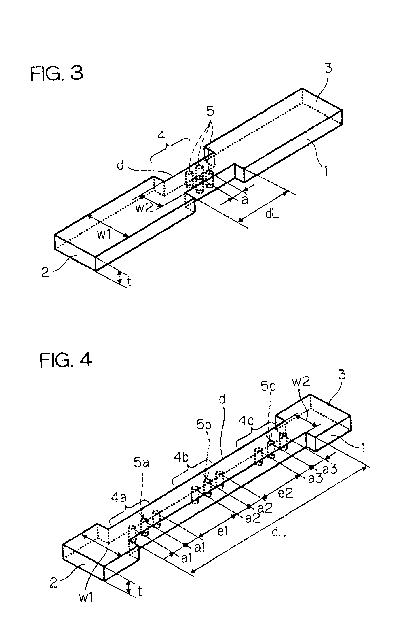
[0093]A dielectric waveguide type filter shown in FIG. 3 was manufactured. The transmittance characteristic of the filter is shown in FIG. 6. Parameters of the filter were as follows. Parameters of the basic dielectric waveguide were the same with those of Example 1. Of the resonator 4, the width of the cutoff waveguide w2=0.8 mm, the length of the cutoff waveguide path dL=2.0 mm, the dielectric constant of the dielectric in the dielectric vias ∈d=20.0, the dielectric via diameter b=φ0.2 mm, and the dielectric via pitch (center distance) a=0.4 mm. Further, the dielectric vias 5 were arranged in a column along the central axis of the cutoff waveguide path d.

[0094]In this case, a characteristic that the resonant frequency is 74.1 GHz and the transmittance frequency band width is 0.9 GHz was obtained, and it proves that such a structure functions as a filter. It is understood in comparison with Example 1 that the transmittance characteristic can be controlled by controlling the positio...

example 3

[0095]A dielectric waveguide type filter shown in FIG. 4 was manufactured. The transmittance characteristic of the filter is shown in FIG. 7. Parameters of the filter were as follows. Parameters of the basic dielectric waveguide were the same with those of Example 1. Of the resonator 4, the width of the cutoff waveguide w2=0.8 mm, the length of the cutoff waveguide path dL=7.2 mm, the dielectric constant of the dielectric vias 5a, 5b, 5c, ∈d=20.0, the dielectric via diameter b=φ0.2 mm, the dielectric via pitches a1, a2, a3=0.5 mm, and the distances between the via groups e1=1.57 mm, e2=1.57 mm. Further, the dielectric via groups of the resonators 4a, 4b, 4c were arranged in a column along the central axis of the cutoff waveguide path respectively. Further, the dielectric via group of the resonators 4 was arranged at a position displaced by 0.03 mm from the central axis of the cutoff waveguide path.

[0096]In this case, a characteristic that the central frequency is 73.3 GHz and the tr...


PUM


Abstract

A cutoff waveguide path is provided in a part of a dielectric waveguide comprising a pair of main conductive layers formed on an upper and a lower surfaces of a dielectric and groups of conductive vias arranged in the direction of signal transmission with a space of a distance less than ½ of a signal wavelength between the conductive vias, and provided in the cutoff waveguide path is a resonator having dielectric vias formed of a dielectric having a higher dielectric constant than that of a dielectric forming the dielectric waveguide. With this construction, a dielectric waveguide type filter easily designed and manufactured can be obtained.

Description

[0001]This application is based on applications Nos. 2000-363695 and 2001-022252 filed in Japan, the content of which is incorporated hereinto by reference.FIELD OF THE INVENTION[0002]The present invention relates to a dielectric waveguide type filter and a dielectric waveguide type branching filter mainly used at high frequencies such as microwaves and millimeter waves and capable of being packaged in an inside of a multi-layered wiring substrate, a semiconductor package, transmitting and receiving module and the like.DESCRIPTION OF THE RELATED ART[0003]Recently, studies on vehicular communication, inter-vehicle radar, wireless LAN and the like used at high frequencies such as microwaves and millimeter waves have been positively progressed. These technologies using high frequencies need a band pass filter capable of passing only high frequency signals of specified frequencies, and a branching filter capable of taking out high frequency signals of specified frequencies.[0004](A) FIG...

Claims


Application Information

Patent Timeline
Patent Type & Authority Patents(United States)
IPC IPC(8): H01P1/208H01P3/12H01P1/213H01P1/20H01P3/00
CPCH01P1/2088H01P1/2138H01P3/121
Inventor UCHIMURA, HIROSHIKITAZAWA, KENJI
Owner KYOCERA CORP
Why Eureka
Try Eureka