Ferroelectric memory and electronic apparatus

a technology of ferroelectric memory and electronic equipment, applied in the field of ferroelectric memory, can solve the problems of difficult to improve the degree of integration in the memory cell and increase the memory capacity, the hysteresis curve angularity is problematic, and it is not possible to control the orientation of the ferroelectric layer, etc., to achieve the effect of low cost, high reliability and small siz

Inactive Publication Date: 2005-08-16
SEIKO EPSON CORP
View PDF16 Cites 8 Cited by
  • Summary
  • Abstract
  • Description
  • Claims
  • Application Information

AI Technical Summary

Benefits of technology

[0035]By providing a ferroelectric memory which is low in cost and has both integration and memory characteristics in the

Problems solved by technology

As single cell therefore has a large area, it was difficult to improve the degree of integration in the memory cell and increase the memory capacity.
It is therefore not possible to control the orientation of the ferroelectric layer, and so, the angles that are formed by the impresse

Method used


Image

  • Ferroelectric memory and electronic apparatus
  • Ferroelectric memory and electronic apparatus
  • Ferroelectric memory and electronic apparatus

Examples


first embodiment

(Device)

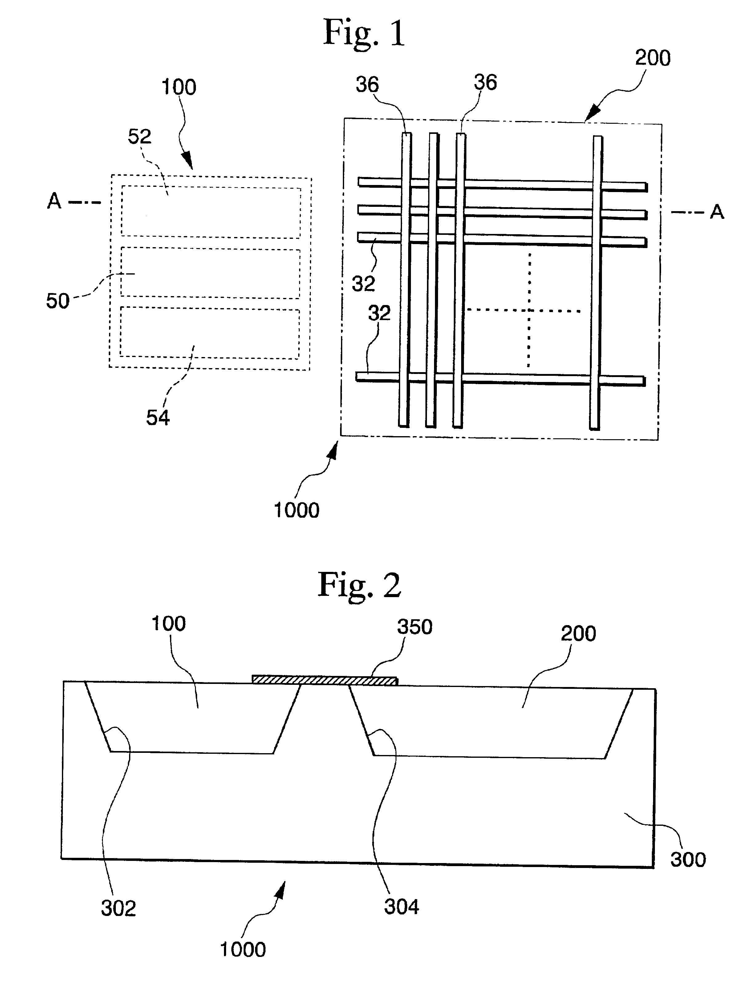
[0045]FIG. 1 is a plan view schematically showing the ferroelectric memory according to the present embodiment. FIG. 2 is a cross section schematically showing the portion of the ferroelectric memory along the line A—A indicated in FIG. 1.

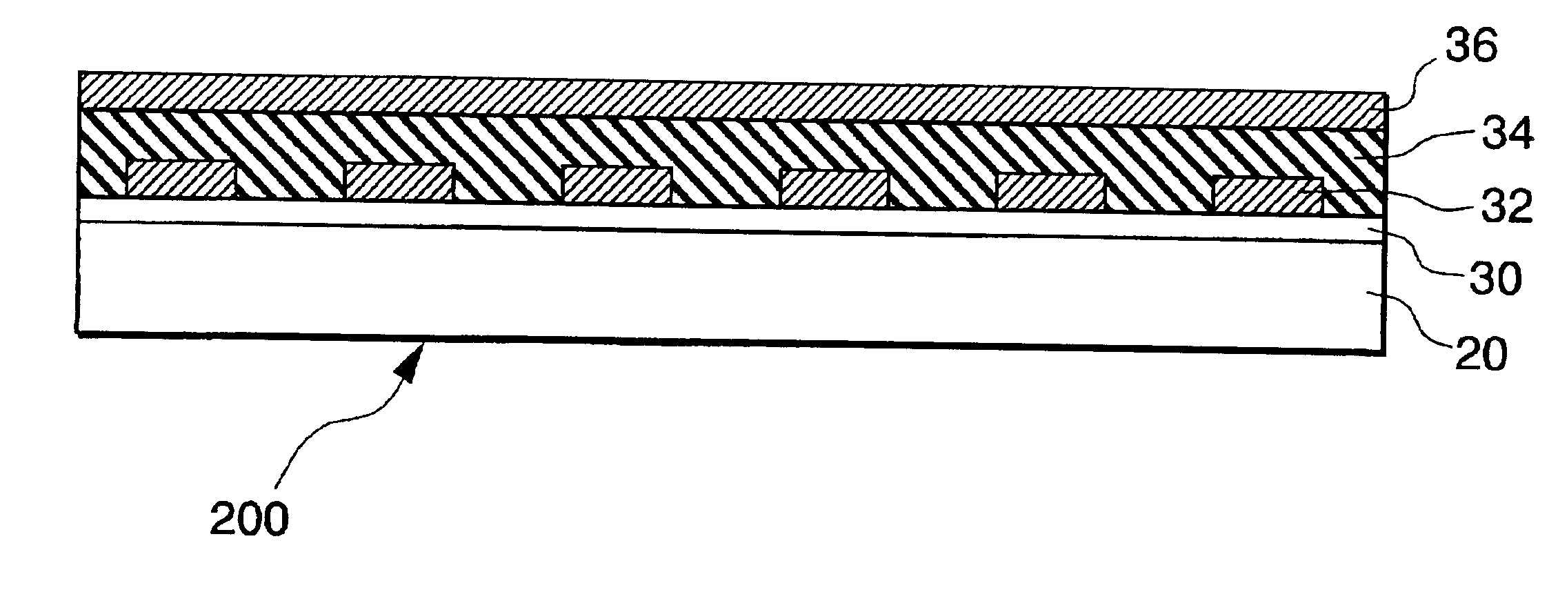
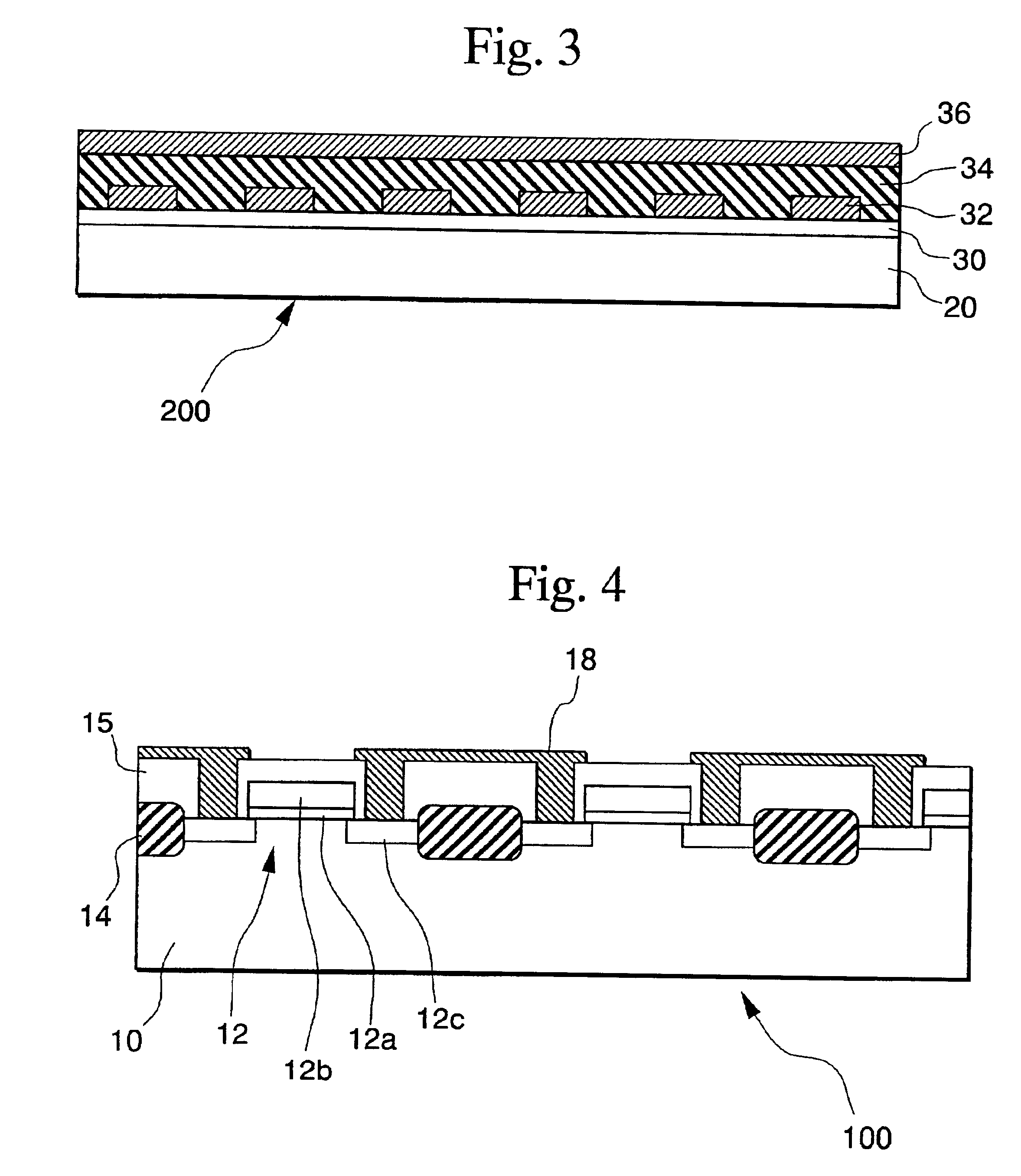
[0046]FIG. 3 is a cross section showing an essential portion of the memory cell array chip of the ferroelectric memory shown in FIG. 1. FIG. 4 is a cross-sectional view showing the structure of the peripheral chip of the ferroelectric memory shown in FIG. 1.

[0047]As shown in FIG. 1, the peripheral circuit and the memory cell array are formed to separate chips in ferroelectric memory 1000 according to the present embodiment. In other words, as shown in FIG. 2, in this ferroelectric memory 1000, peripheral circuit chip 100 and memory cell array chip 200 separately engage in concavity 302 and concavity 304 which are formed at specific sites in assembly base 300.

[0048]In memory cell array chip 200, as shown in FIG. 3, a buffer layer 30 is forme...

second embodiment

[0066]FIG. 5 is a plan view schematically showing the ferroelectric memory according to the present embodiment. FIG. 6 is a cross section schematically showing the ferroelectric memory shown in FIG. 5.

[0067]In ferroelectric memory 2000 according to the present embodiment, peripheral circuit chip 100 and memory cell array chip 200 are laminated and engaged in this state in concavity 310 that is formed at a specific position in mounting base 300.

[0068]Ferroelectric memory 2000 according to this embodiment can be formed using the conventionally known FSA method discussed above. Specifically, a FSA method is employed to engage peripheral circuit 100 in the bottom of concavity 310 of assembly base 300. Next, a first connective wiring layer 360 having a specific pattern is formed along the surface of peripheral circuit chip 100 and assembly base 300. Next, an insulating layer 320 is formed that also functions as a flattening layer. A FSA method is then used to engage memory cell array chi...

third embodiment

[0070]FIG. 7 is a cross section schematically showing the ferroelectric memory according to this embodiment.

[0071]Ferroelectric memory 3000 according to this embodiment has a structure in which a plurality of peripheral circuit chips 100 and memory cell array chips 200 are alternately layered inside concavity 310 that is formed in mounting base 300.

[0072]A conventionally known FSA method can be employed to form ferroelectric memory 3000 according to this embodiment. Specifically, a FSA method is employed to engage a peripheral circuit 100 in the bottom of concavity 310 in assembly base 300. Next, a first connective wiring layer 360 having a specific pattern is formed along the surface of peripheral circuit chip 100 and mounting base 300. Next, an insulating layer 320 is formed that also functions as a planarizing layer. A FSA method is then used to engage a memory cell array chip 200 inside upper concavity 312 which is formed by the walls of insulating layer 320. A second connective...


PUM


Abstract

The present invention relates to a ferroelectric memory having a matrix-type memory cell array which has a superior degree of integration, in which the angularity of the ferroelectric layer's hysteresis curve is improved, the production yield is increased and costs are reduced.
A ferroelectric memory having improved angularity in the hysteresis curve, and superior memory characteristics, production yield and costs is realized as follows. Namely, a peripheral circuit chip and a memory cell array chip are engaged onto an inexpensive assembly base 300 such as glass or plastic. In memory cell array chip 200, a ferroelectric layer is made to undergo epitaxial growth on to a Si single crystal via a buffer layer and first signal electrode. As a result, a ferroelectric memory can be realized which has improved angularity in the hysteresis curve and superior memory characteristics, production yield, and cost.

Description

BACKGROUND OF THE INVENTION[0001]1. Field of the Invention[0002]The present invention relates to a ferroelectric memory, and more specifically to a sample matrix-type ferroelectric memory that uses only a ferroelectric capacitor and does not have a cell transistor. The present invention further relates to an electronic apparatus provided with this ferroelectric memory.[0003]2. Description of Related Art[0004]Ferroelectric memory has undergone rapid development in recent years as a form of nonvolatile memory employing a ferroelectric substance. Typically, a ferroelectric capacitor is formed by employing an oxidized ferroelectric material as the capacitor insulating film, and is used as a non-volatile memory by storing data according to the polarization direction of the ferroelectric capacitor.[0005]In the usual ferroelectric memory, the peripheral circuit for selectively carrying out the writing and reading out of data to and from a memory cell and the memory cell are formed in close...

Claims


Application Information

Patent Timeline
IPC IPC(8): H01L27/105H01L21/8246G11C11/22
CPCH01L27/105
Inventor HIGUCHI, TAKAMITSUIWASHITA, SETSUYAMIYAZAWA, HIROMUHASEGAWA, KAZUMASANATORI, EIJI
Owner SEIKO EPSON CORP
Why Eureka
Try Eureka