Universal substrate holder for treating objects in fluids

a technology of fluid treatment and substrate, applied in the direction of chucks, manufacturing tools, mechanical equipment, etc., can solve the problems of voids in interconnects and plugs formed, insufficient thick seed layers to carry current to the bottom of high aspect ratio features, and inconformity of copper deposition by electroplating side walls, etc., to achieve the effect of simple construction

Inactive Publication Date: 2005-08-30
LAM RES CORP
View PDF18 Cites 19 Cited by
  • Summary
  • Abstract
  • Description
  • Claims
  • Application Information

AI Technical Summary

Benefits of technology

[0022]It is an object of the invention to provide a substrate holder for treatment of substrates in liquids, which possesses universality and is capable of selectively providing treatment of substrates from both sides or only from the face side, while protecting the backside of the substrate from the effect of the process solution. It is another object to provide a substrate holder of the aforementioned type, which is simple in construction and utilizes one and the same element for two functions, such as supporting the substrate and controlling operation of substrate clamping elements.
[0023]A universal substrate holder of the invention for treating wafer substrates in liquids, e.g., for use in, electroless deposition apparatuses, has a housing with a bowl which is sealed from the housing and can be filled with a deposition solution, rinsing solution, cleaning solution, or the like. The holder is provided with a shaft, one end of which protrudes into the bowl and the opposite end is connected to a rotary drive. A rod is slidingly inserted into the central opening of the shaft so that it can slide inside but cannot rotate relative to the shaft. The end of the shaft that protrudes into the bowl supports a base platform for the subs...

Problems solved by technology

One drawback associated with copper deposition by electroplating is the fact that for very small features on microelectronic workpieces (sub 0.1 micron features), copper deposition by electroplating can lack conformity with the side walls of high aspect ratio vias and trenches, and can produce voids in the formed interconnects and plugs (vias).
This is often due to the non-conformity of the copper seed layer deposited by PVD or CVD.
As a result, the seed layer may not be thick enough to carry the current to the bottom of high aspect ratio features.
A main disadvantage of the substrate holder of U.S....

Method used


Image

  • Universal substrate holder for treating objects in fluids
  • Universal substrate holder for treating objects in fluids
  • Universal substrate holder for treating objects in fluids

Examples


Embodiment Construction

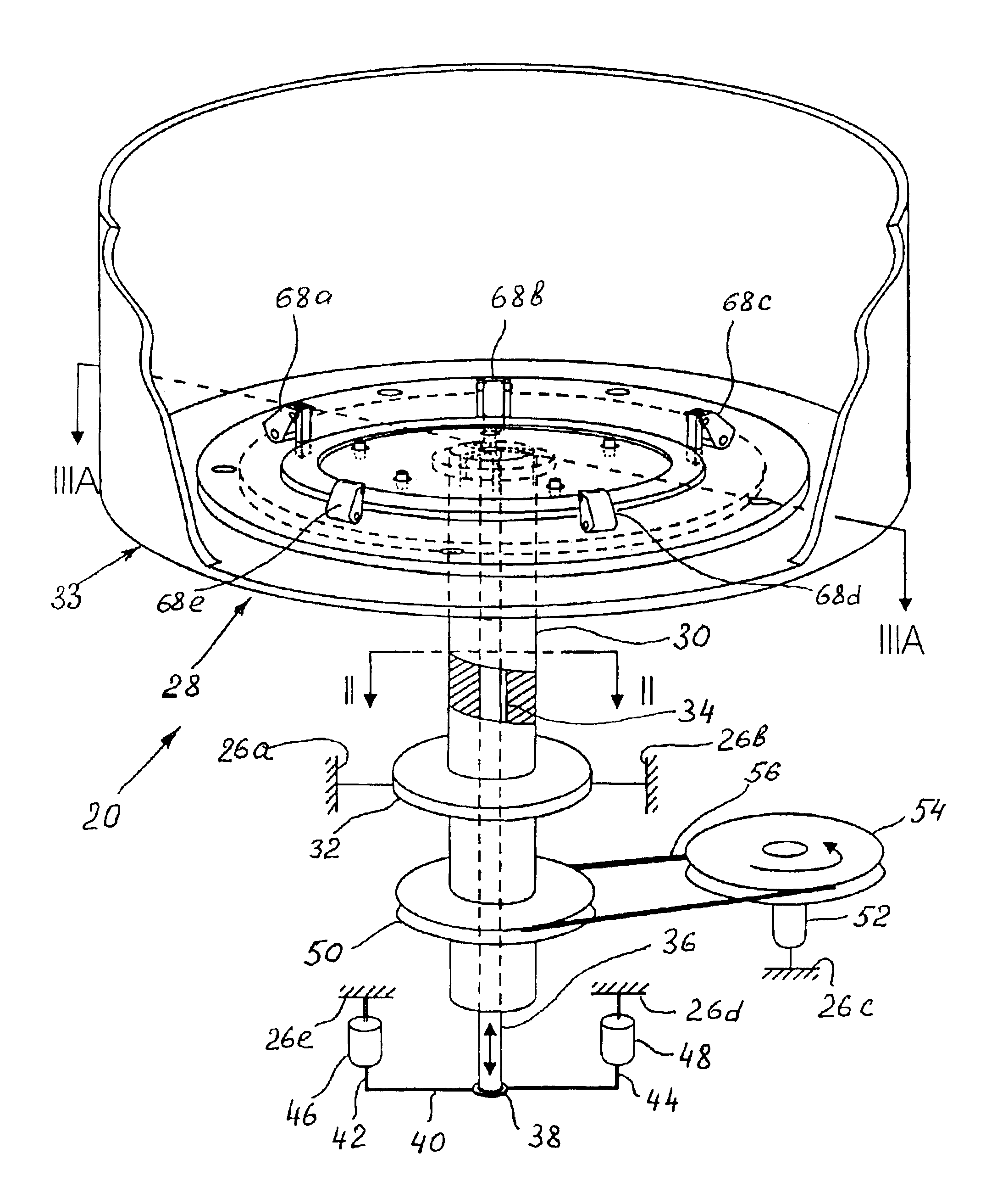
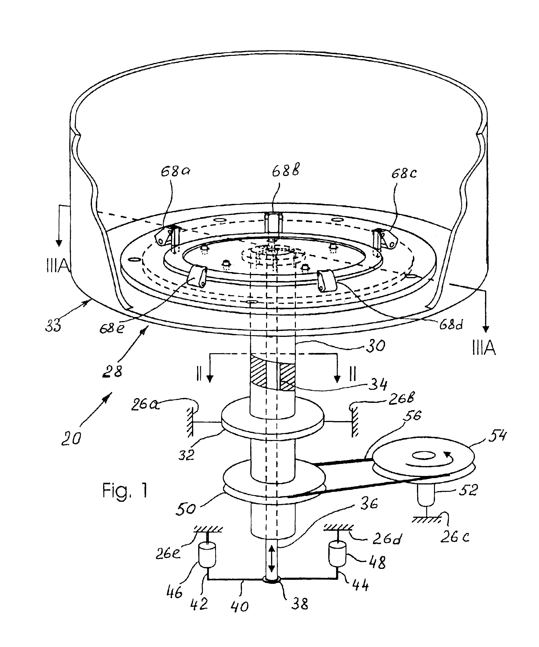
[0032]A general three-dimensional view of the part of an electroless deposition apparatus that incorporates the substrate holder of the invention is shown in FIG. 1. The apparatus, which in general is designated by reference numeral 20 is shown without a housing and with a part of a bowl removed for exposing inner parts of the substrate holder. It is also understood that reference to the electroless deposition apparatus is given only as an example and that any other apparatus or machine for treating flat objects in a fluid may incorporate the holder of the invention.

[0033]The apparatus 20 has a housing, which in the embodiment of FIG. 1 is shown conventionally by lines with hatchings 26a, 26b, 26c, 26d, and 26e. It is assumed that the housing supports a bowl 28 with an open top side.

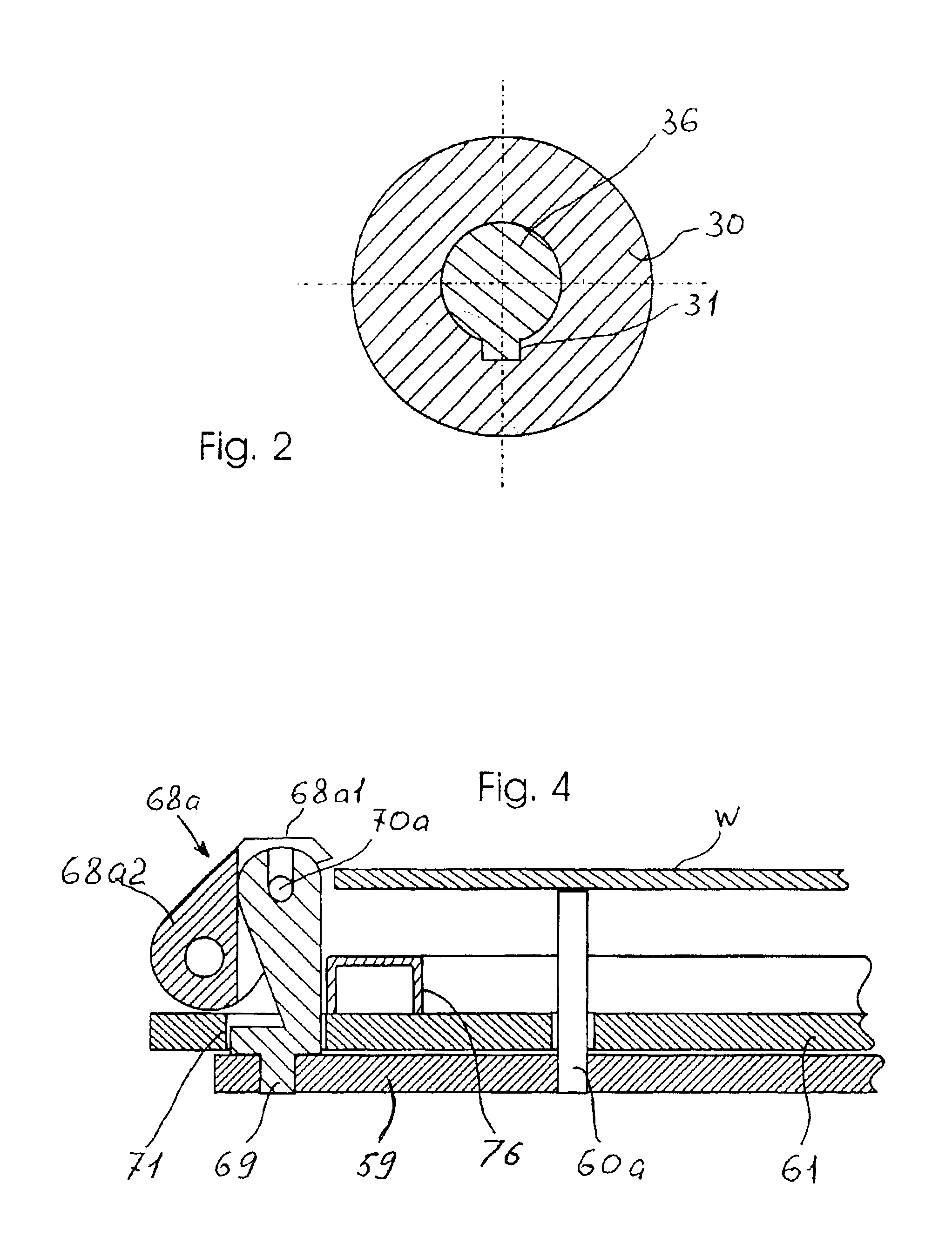
[0034]The parts and elements described below constitute a substrate holder, which as a whole is designated by reference numeral 33. More specifically, the substrate holder 33 has a vertical shaft 30, whi...


PUM


Abstract

A universal substrate holder of the invention for treating wafer substrates in liquids is provided with a shaft and a rod slidingly inserted into the central opening of the shaft. The end of the shaft that protrudes into the bowl supports a base platform for the substrate, while the end of the rod that protrudes into the bowl has radial arms that rigidly support an annular plate with pins that can pass through the opening of the base platform so that they can support the substrate above the surface of the platform. The annular plate supports clamping jaws made in the form of two-arm levers with shorter arms and longer arms. The longer arms are heavier and therefore in the stationary state of the holder keep the jaws turned into an open position. When the shaft begins to rotate, the jaws are turned under the effect of centrifugal forces into positions of clamping the substrate with the shorter arms. When the rod is pulled down, the ends of the longer arms come into contact with the base platform and are turned into the clamping position. The substrate holder of the invention allows clamping and releasing of the substrate in positions of the substrate above the platform and in a position of the substrate on the base substrate, when the backside of the substrate is inaccessible to the process liquid.

Description

FIELD OF THE INVENTION[0001]The present invention relates to semiconductor production equipment, in particular, to a universal substrate holder or chuck for holding semiconductor substrates during treatment in fluids, e.g., to a wafer substrate chuck used in an apparatus for electroless deposition of materials on semiconductor substrates.BACKGROUND OF THE INVENTION[0002]Manufacturing of semiconductor devices, in particular integrated circuits having multiple-layered structures with various metal and non-metal layers laminated on a semiconductor substrate, typically involves applications, of several metal layers onto a substrate or onto other previously deposited layers. These layers may have a complicated planer topology since these layers may constitute thousands of individual devices, which in combination form an integrated circuit or so-called “chip”. Modern chips may have metal or dielectric layers with thicknesses from tens of Angstroms to fractions of a micron.[0003]It is unde...

Claims


Application Information

Patent Timeline
IPC IPC(8): B23B31/14B23B31/12B23B31/18H01L21/00H01L21/687
CPCB23B31/14B23B31/18H01L21/67126H01L21/68728Y10T279/247Y10T279/18Y10T279/24H01L21/68707B23B31/142
Inventor IVANOV, IGOR C.ZHANG, JONATHAN WEIGUO
Owner LAM RES CORP
Why Eureka
Try Eureka