On-chip inductor having a square geometry and high Q factor and method of manufacture thereof

a technology of on-chip inductor and square geometry, which is applied in the direction of transformer/inductance details, semiconductor devices, coils, etc., can solve the problems of large ic footprint, violation of foundry rules, and impracticality of octagonal inductor, so as to reduce the impedance of conductive winding, reduce the capacitance value, and increase the quality factor

Inactive Publication Date: 2005-08-30
AVAGO TECH INT SALES PTE LTD
View PDF3 Cites 13 Cited by
  • Summary
  • Abstract
  • Description
  • Claims
  • Application Information

AI Technical Summary

Benefits of technology

[0007]These needs and others are substantially met by the on-chip inductor and / or on-chip transformer disclosed herein. Such an on-chip inductor includes a dielectric layer and a conductive winding on the dielectric layer. The conductive winding has a substantially square geometry and has at least its exterior corners geometrically shaped to reduce impedance of the conductive winding at a particular operating frequency. Since the quality factor of an on-chip inductor is inversely proportional to the effective series impedance of the inductor at an operating frequency, by reducing the effective series impedance, the quality factor is increased. In addition, the inductor has lower capacitance values in comparison to substantially equal inductors that do not practice the present invention, thus allowing the inductor of the present invention to have a higher self-resonance.

Problems solved by technology

As is known, a circular trace pattern for an on-chip inductor theoretically has a greater Q factor than a square or rectangular trace pattern of similar inductance, but has a larger IC footprint and violates foundry rules.
In some instances, an octagonal inductor is impractical due to its size and yet a square or rectangular on-chip inductor is impractical due to its low quality factor.

Method used


Image

  • On-chip inductor having a square geometry and high Q factor and method of manufacture thereof
  • On-chip inductor having a square geometry and high Q factor and method of manufacture thereof
  • On-chip inductor having a square geometry and high Q factor and method of manufacture thereof

Examples


Embodiment Construction

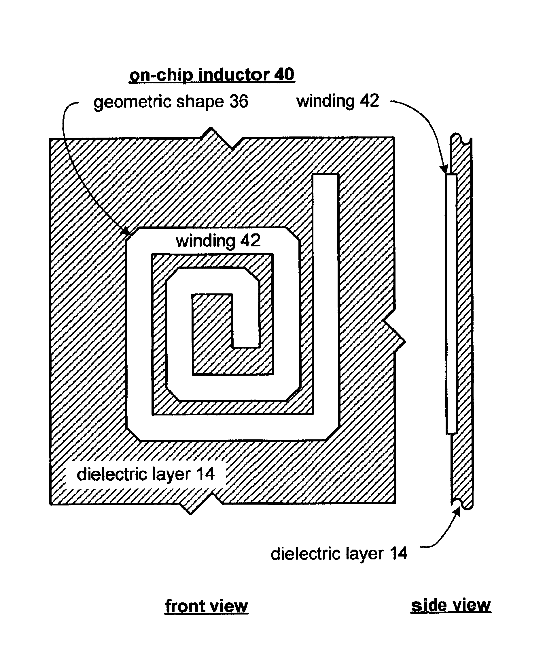
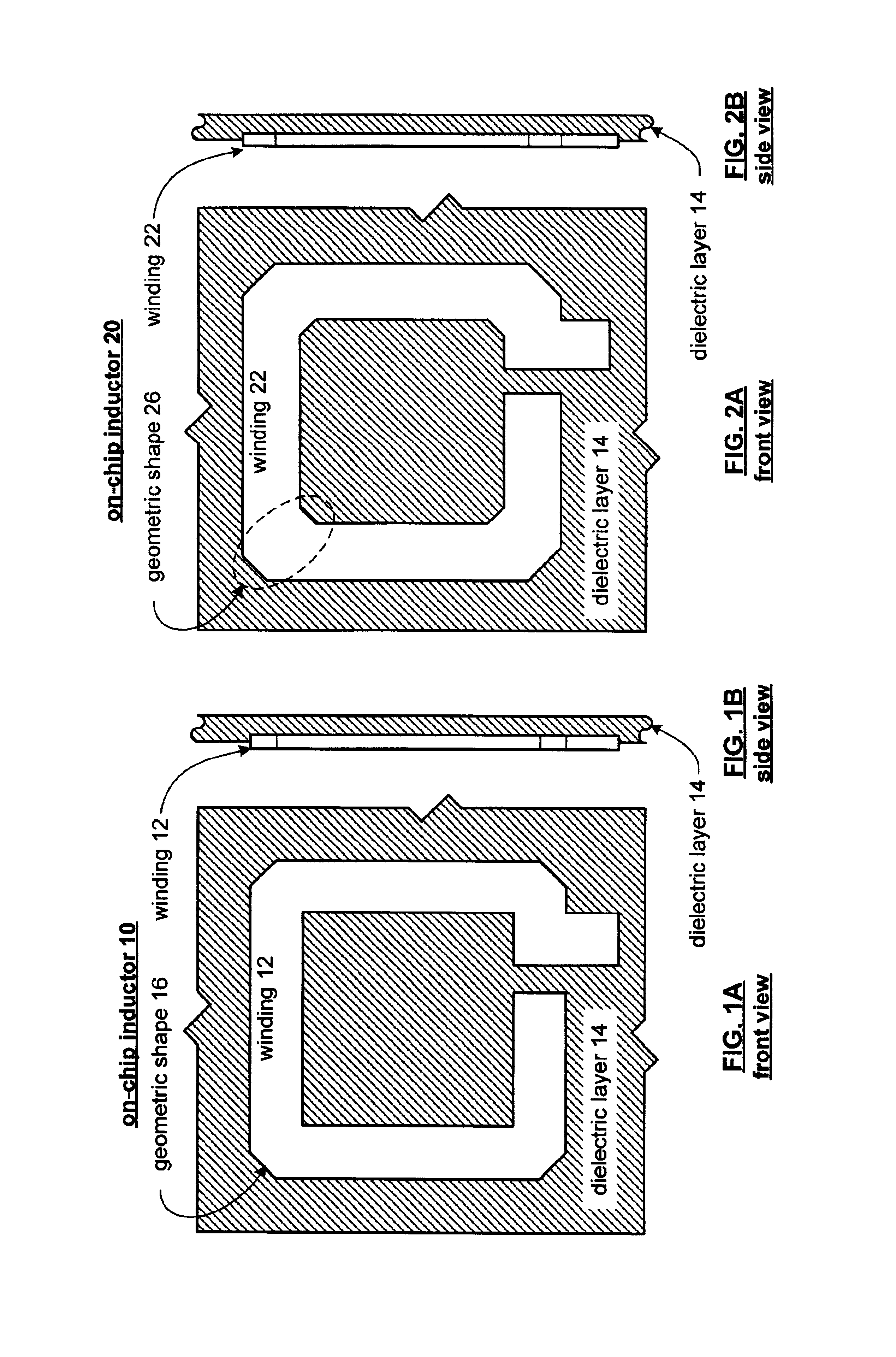
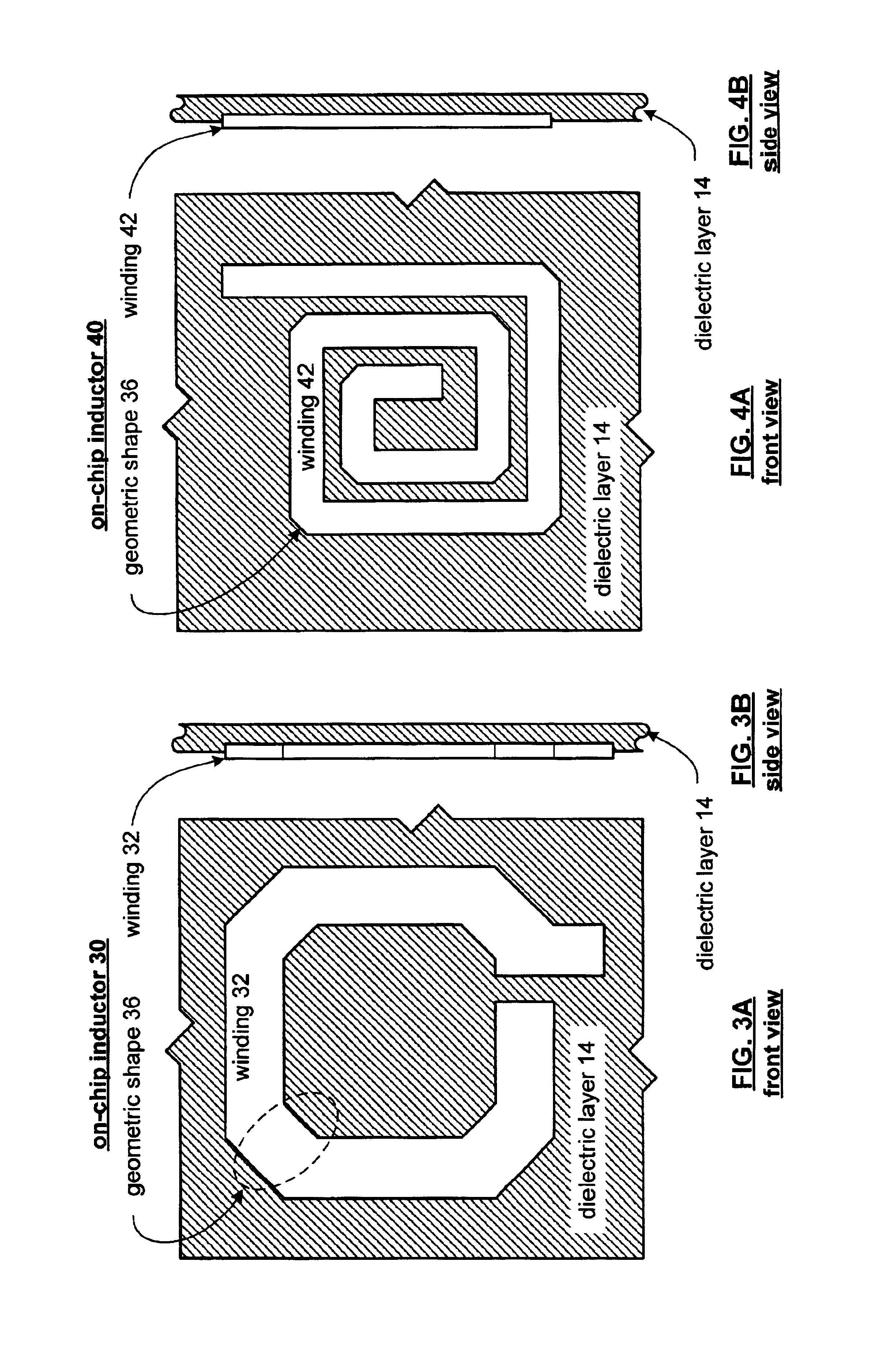
[0019]FIGS. 1A and 1B illustrate an on-chip inductor 10 that includes a winding12 on a dielectric layer 14. The winding 12 includes geometric shaping 16 at its exterior corners. As illustrated, winding 12 has a substantially square shape and may include one or more turns on one or more dielectric layers. By including the geometric shaping 16, the effective impedance at operating frequencies (e.g., 2.4 gigahertz) is reduced, thereby increasing the quality factor of on-chip inductor 10.

[0020]In general, the inductance value of an on-chip inductor is dependent on the length of the interior edge of the metalization (i.e., the interior edge of winding 12) where the current tends to concentrate. Accordingly, the interior diameter of the inductor is the deciding factor for size minimization. As has been demonstrated in simulations, the highest current density is distributed on the interior edge of an inductor and gives the dominate contribution to the inductance. Note that the simulations ...


PUM

PropertyMeasurementUnit
interior angleaaaaaaaaaa
exterior angleaaaaaaaaaa
interior angleaaaaaaaaaa

Abstract

An on-chip inductor and / or on-chip transformer includes at least one dielectric layer and at least one conductive winding on the at least one dielectric layer. The conductive winding has a substantially square geometry and has at least its exterior corners geometrically shaped to reduce impedance of the conductive winding at a particular operating frequency. Since the quality factor of an on-chip inductor is inversely proportional to the effective series impedance of an inductor at an operating frequency, by reducing the effective series impedance, the quality factor is increased.

Description

TECHNICAL FIELD OF THE INVENTION[0001]This invention relates generally to integrated circuits and more particularly to on-chip inductors and on-chip transformers.BACKGROUND OF THE INVENTION[0002]Integrated circuits (IC's) are known to include a substrate, one or more dielectric layers on the substrate, and one or more metal layers supported by a corresponding dielectric layer. The metal layers are fabricated in such a way to produce on-chip components such as resistors, transistors, capacitors, inductors, et cetera. How an on-chip component is fabricated and the physical limits placed on on-chip components are dictated by the technology used and foundry rules governing such technology.[0003]For example, CMOS technology is readily used for cost effective integrated circuits. Foundries that manufacture CMOS integrated circuits provide rules governing the number of dielectric layers, number of metal layers, metal track sizes, spacing between metal tracks, angular bends of metal tracks,...

Claims


Application Information

Patent Timeline
Patent Type & Authority Patents(United States)
IPC IPC(8): H01L27/08
CPCH01L27/08Y10T29/49071Y10T29/4902Y10T29/49073
Inventor CONTOPANAGOS, HARRYKYRIAZIDOU, SISSY
Owner AVAGO TECH INT SALES PTE LTD
Why Eureka
Try Eureka