Current sensing method and apparatus particularly useful for a memory array of cells having diode-like characteristics

a memory array and current sensing technology, applied in static storage, digital storage, instruments, etc., can solve the problems of large leakage current between unselected bit lines and unselected word lines within the array, long sense delay, and difficult sensing of memory cells in the array, so as to eliminate leakage current

Inactive Publication Date: 2005-08-30
SANDISK TECH LLC
View PDF41 Cites 24 Cited by
  • Summary
  • Abstract
  • Description
  • Claims
  • Application Information

AI Technical Summary

Benefits of technology

[0010]An improved sensing method biases a selected bit line at a particular voltage, and the current through the selected memory cell is sensed while the selected bit line voltage is generally maintained at the particular voltage. In a preferred embodiment particularly suitable for an antifuse memory cell, the bias on a selected bit line is changed by 1 volt or more relative to its bias when previously unselected. The particular voltage for the selected bit line is preferably chosen to be substantially equal to the unselected word line voltage to substantially eliminate leakage current through half-selected memory cells on the selected bit line. By biasing the unselected word lines and bit lines in accordance with the invention, negligible leakage currents flow to or from the selected word line and bit line, and the bit line current which is sensed arises largely from only the current through the selected memory cell.
[0011]In other embodiments, the voltage clamped bit line sensing may be combined with a noise detection line in the memory array, to reduce the effect of coupling from unselected word lines to the selected bit line. In a preferred embodiment, a three-dimensional memory array having bit lines on more than one layer includes at least one noise detection line associated with each layer of bit lines. A sensing circuit is connected to a selected bit line and to its associated noise detection line.

Problems solved by technology

Moreover, particularly with memory cells (i.e., memory elements) that include diodes, there are frequently large leakage currents between unselected bit lines and unselected word lines within the array.
These characteristics make sensing a memory cell in the array more difficult.
The large capacitance loading on a selected bit line delays the development of a voltage signal on the selected bit line, causing long sense delays.
This is especially true in diode arrays because the current available from each memory cell is usually very small.
Also, developing a signal on a particular bit line may couple noise into adjacent bit lines, which reduces the sensing margins available and detracts from reliable sensing.
Leakage currents may consequently flow between the unselected bit lines and unselected word lines during sensing, and may result in small voltage perturbations on the unselected word lines.
Even these small voltage variations may couple very strongly into the bit line being sensed, and make sensing more difficult.
All of these are especially problematic in high density, large capacity memory arrays because the fan out on the memory lines, particularly the bit lines, may be as large as 512 or more and the cell current is usually very small.
Currently, such memories are limited in their performance and may have lower internal signal margins which can potentially cause significant manufacturing difficulty.

Method used


Image

  • Current sensing method and apparatus particularly useful for a memory array of cells having diode-like characteristics
  • Current sensing method and apparatus particularly useful for a memory array of cells having diode-like characteristics
  • Current sensing method and apparatus particularly useful for a memory array of cells having diode-like characteristics

Examples


Embodiment Construction

[0028]In the interest of clarity, not all of the routine features of the implementations described herein are shown and described. It will, of course, be appreciated that in the development of any such actual implementation, numerous implementation-specific decisions must be made in order to achieve the developer's specific goals, such as compliance with application- and business-related constraints, and that these specific goals will vary from one implementation to another and from one developer to another. Moreover, it will be appreciated that such a development effort might be complex and time-consuming, but would nevertheless be a routine undertaking of engineering for those of ordinary skill in the art having the benefit of this disclosure.

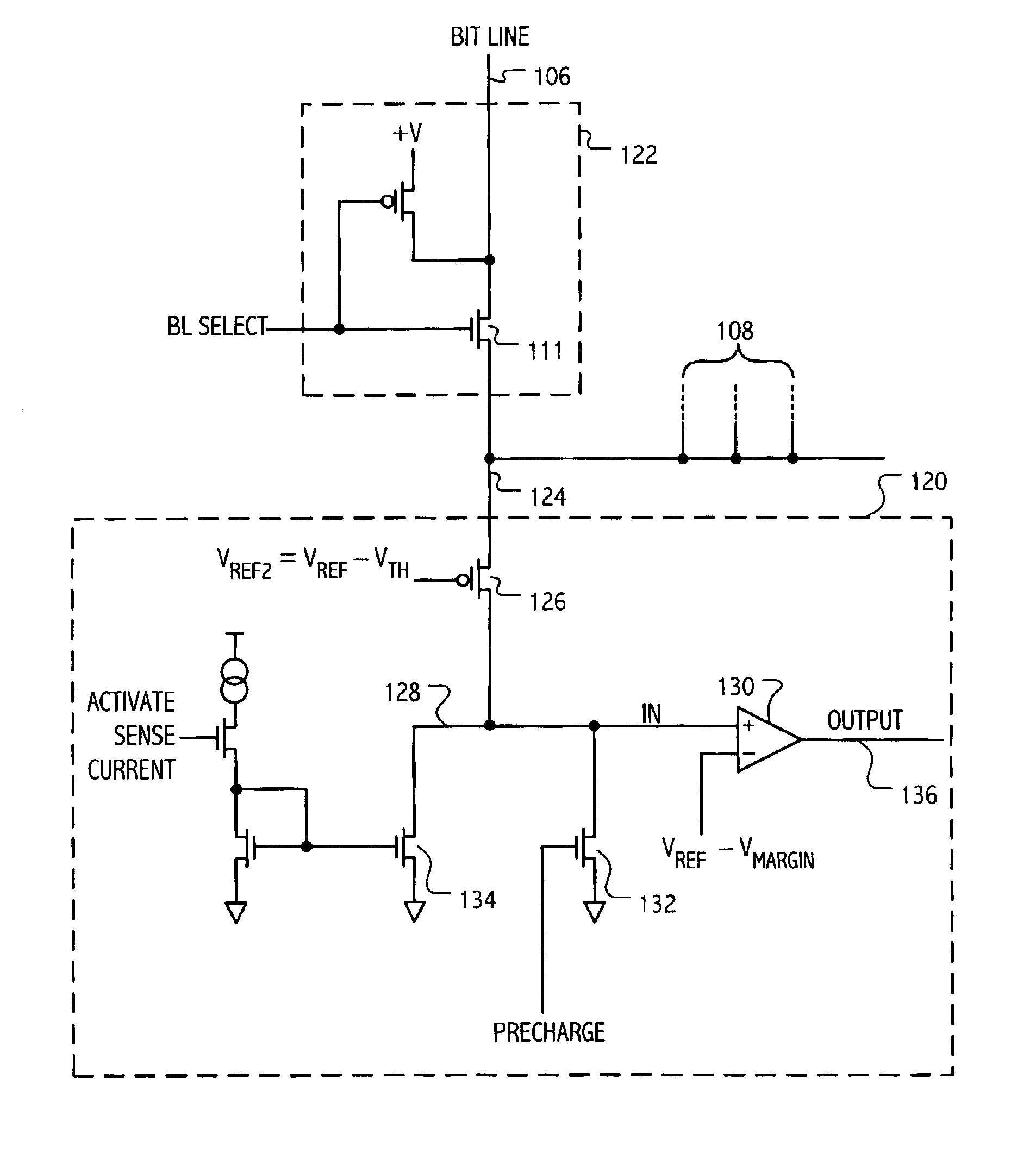
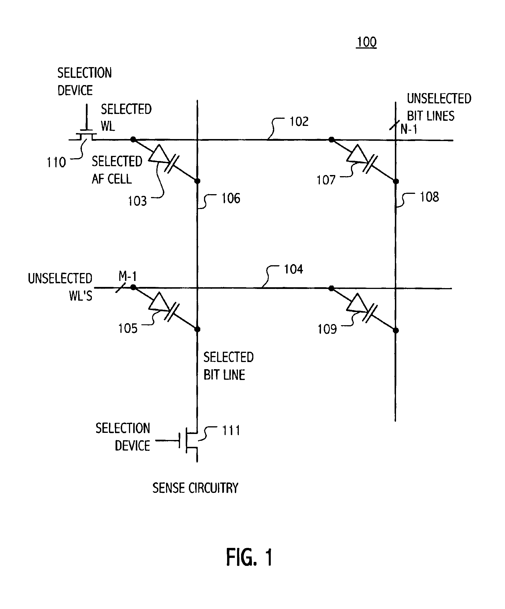
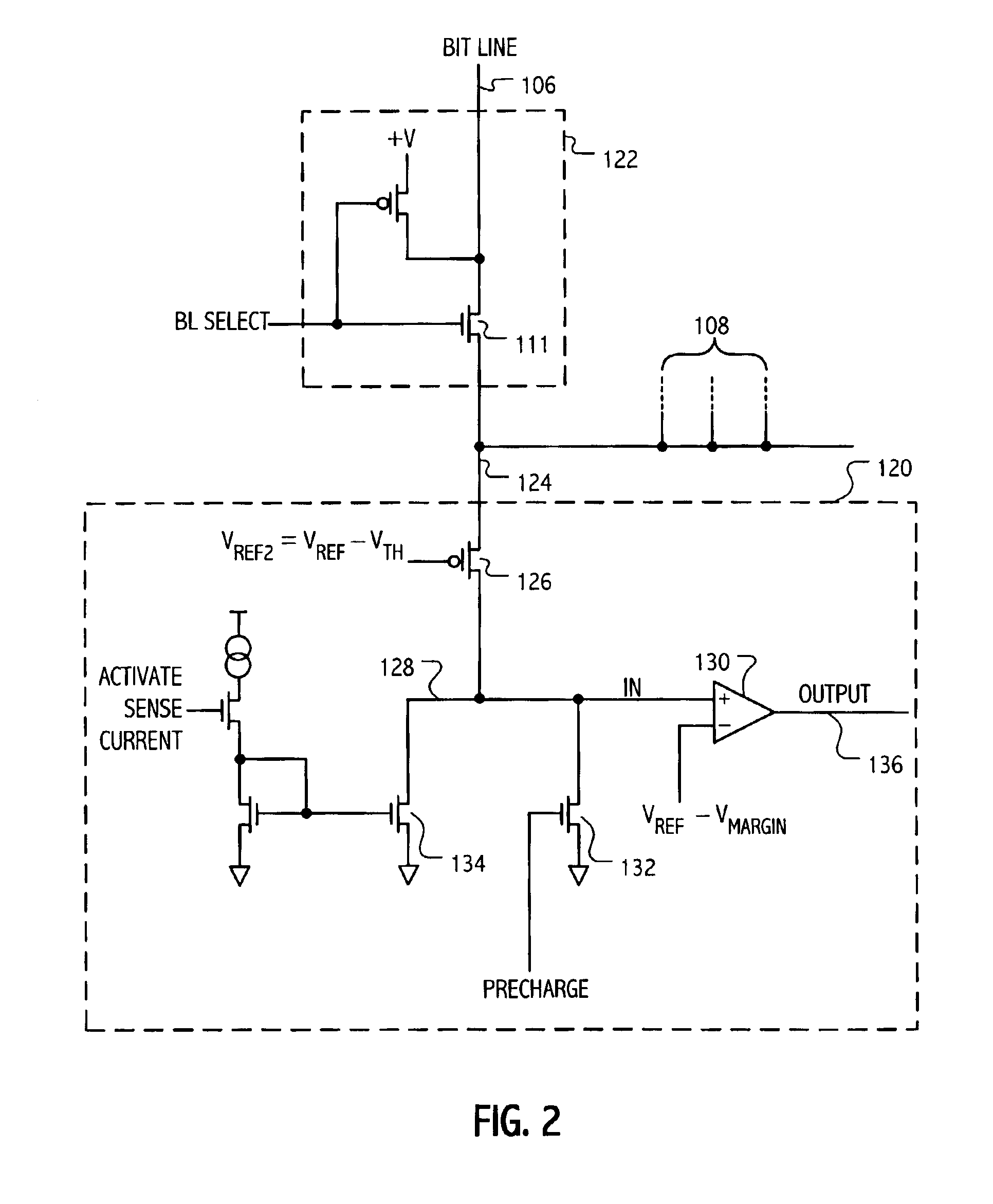
[0029]Referring now to FIG. 1, one layer of a diode stack-type memory array 100 is depicted, showing a selected word line 102, a group of unselected word lines 104 (i.e., M-1 unselected word lines represented by a single line labeled 104), a ...


PUM


Abstract

A memory array includes a sensing circuit for sensing bit line current while keeping the voltage of the selected bit line substantially unchanged. The word lines and bit lines are biased so that essentially no bias voltage is impressed across half-selected memory cells, which substantially eliminates leakage current through half-selected memory cells. The bit line current which is sensed arises largely from only the current through the selected memory cell. A noise detection line in the memory array reduces the effect of coupling from unselected word lines to the selected bit line. In a preferred embodiment, a three-dimensional memory array having a plurality of rail-stacks forming bit lines on more than one layer, includes at least one noise detection line associated with each layer of bit lines. A sensing circuit is connected to a selected bit line and to its associated noise detection line.

Description

CROSS-REFERENCE TO RELATED APPLICATIONS[0001]This application is a divisional of Prior application Ser. No. 09 / 896,468, filed Jun. 29, 2001, which claims the benefit of the following U.S. provisional applications, each of which was filed on Mar. 21, 2001: U.S. Provisional Application No. 60 / 277,794; U.S. Provisional Application No. 60 / 277,815; and U.S. Provisional Application No. 60 / 277,738. Each of the above-referenced applications is hereby incorporated by reference.BACKGROUND OF THE INVENTION[0002]1. Field of the Invention[0003]The present invention relates to high-density semiconductor memories, particularly those having memory cells exhibiting diode-like conduction characteristics, and more particularly, to a three-dimensional passive element memory array and support circuits useful therewith.[0004]2. Description of Related Art[0005]Three-dimensional cross-point memory arrays achieve high density, but also must deal with several attributes of such a dense structure. There is a ...

Claims


Application Information

Patent Timeline
Patent Type & Authority Patents(United States)
IPC IPC(8): G11C8/10G11C5/02G11C7/18G11C7/06G11C8/08G11C7/00G11C8/00G11C17/14G11C17/18
CPCG11C5/025G11C7/062G11C7/067G11C7/18G11C8/08G11C8/10G11C17/18G11C2207/063
Inventor SCHEUERLEIN, ROY E.
Owner SANDISK TECH LLC
Why Eureka
Try Eureka