Ideal operational amplifier layout techniques for reducing package stress and configurations therefor

a technology of operational amplifiers and layout techniques, applied in pulse manipulation, pulse techniques, instruments, etc., can solve problems such as differential voltage (vd), large input offset voltage (vio) variance, and inacceptable yield losses, and achieve the effect of reducing package stress

Inactive Publication Date: 2005-09-06
TEXAS INSTR INC
View PDF13 Cites 21 Cited by
  • Summary
  • Abstract
  • Description
  • Claims
  • Application Information

AI Technical Summary

Problems solved by technology

Assembly induced package stress is the key factor behind many assembly and test (A / T) yield problems for operational amplifier devices.
The contracting of the compound causes stress on the active components of the op-amp, which creates large input offset voltage (VIO) variances.
The wide swings in VIO introduce, in some cases, unacceptable yield losses during the final test.
Further, an input offset mismatch in the input stage (i.e., transistors and other components) during the fabrication of the silicon die creates effects that produce a mismatch of the bias currents flowing through the input stage, which results in a differential voltage (Vd).
This causes the output signal to be unrecognizable from the signal being amplified.
In most analog systems, this type of DC error is the basic limitation on the solution of the system.
Typically, the predominant causes of offset error, from a process viewpoint, lie in the emitter-coupled transistor pair.
Package shift lowers the input offset voltage precision of the device, which raises test yield issues.
However, there is no existing solution that provides a design layout recommendation, which takes “package shift” into consideration even before producing the material.

Method used


Image

  • Ideal operational amplifier layout techniques for reducing package stress and configurations therefor
  • Ideal operational amplifier layout techniques for reducing package stress and configurations therefor
  • Ideal operational amplifier layout techniques for reducing package stress and configurations therefor

Examples


implementation embodiments

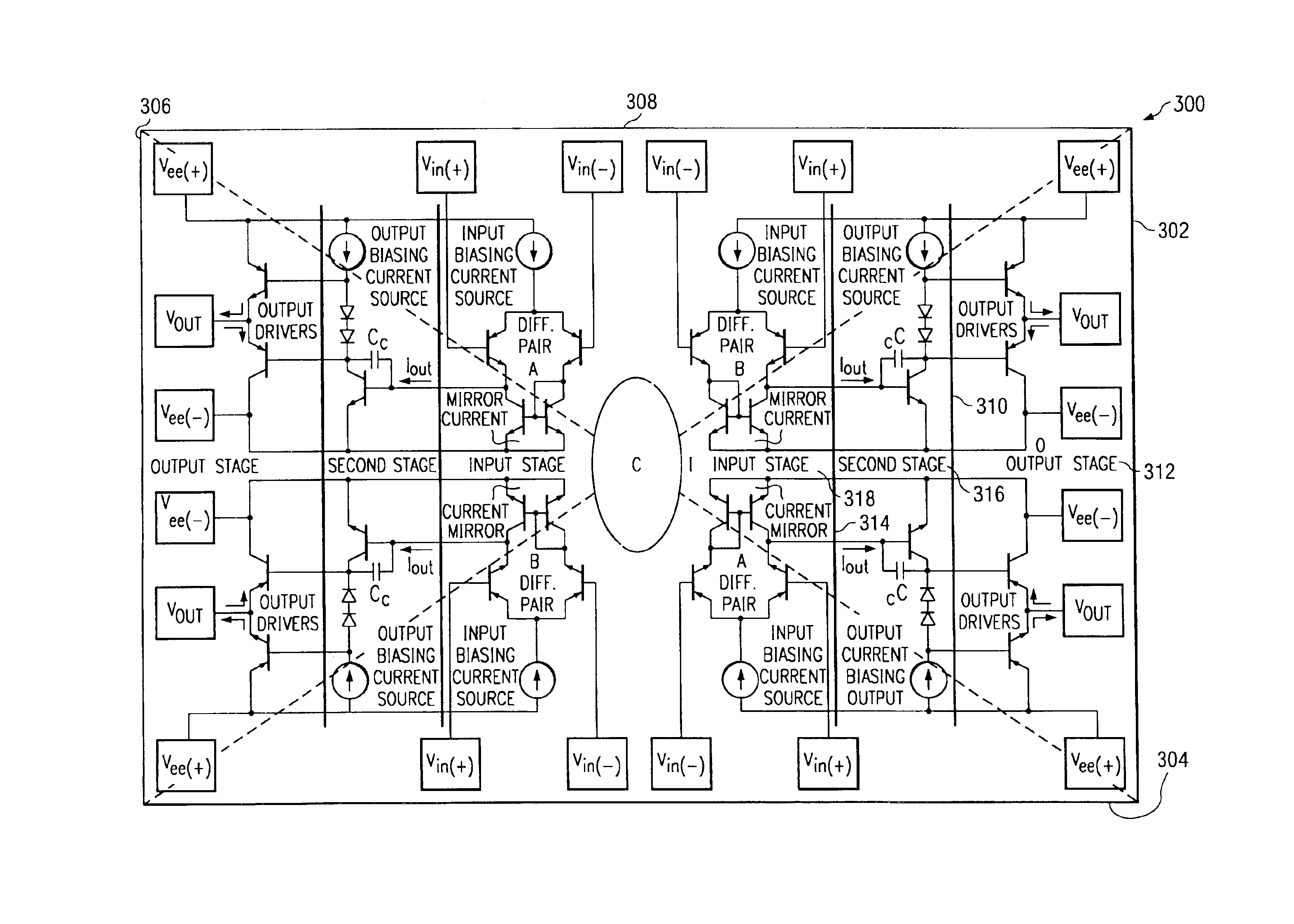
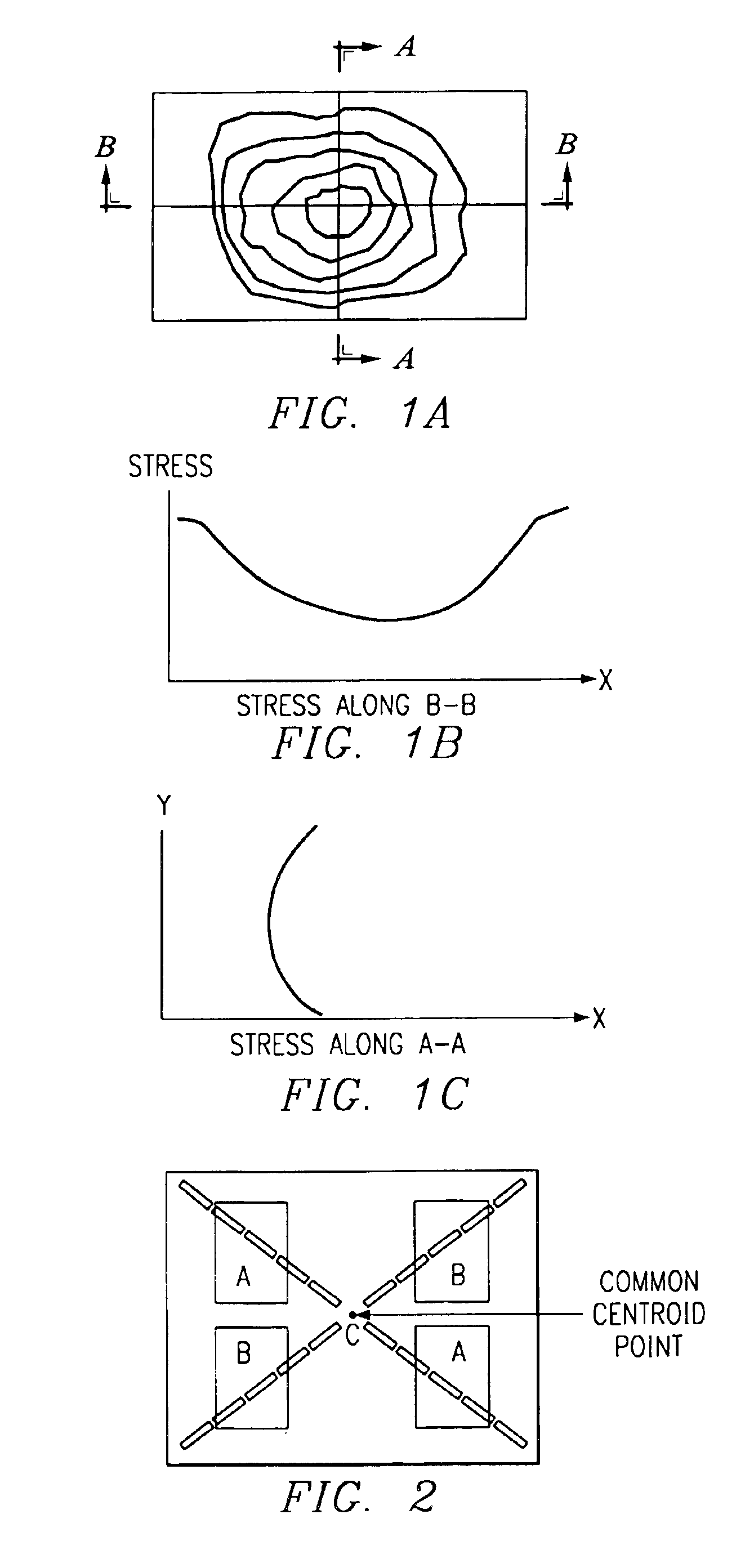
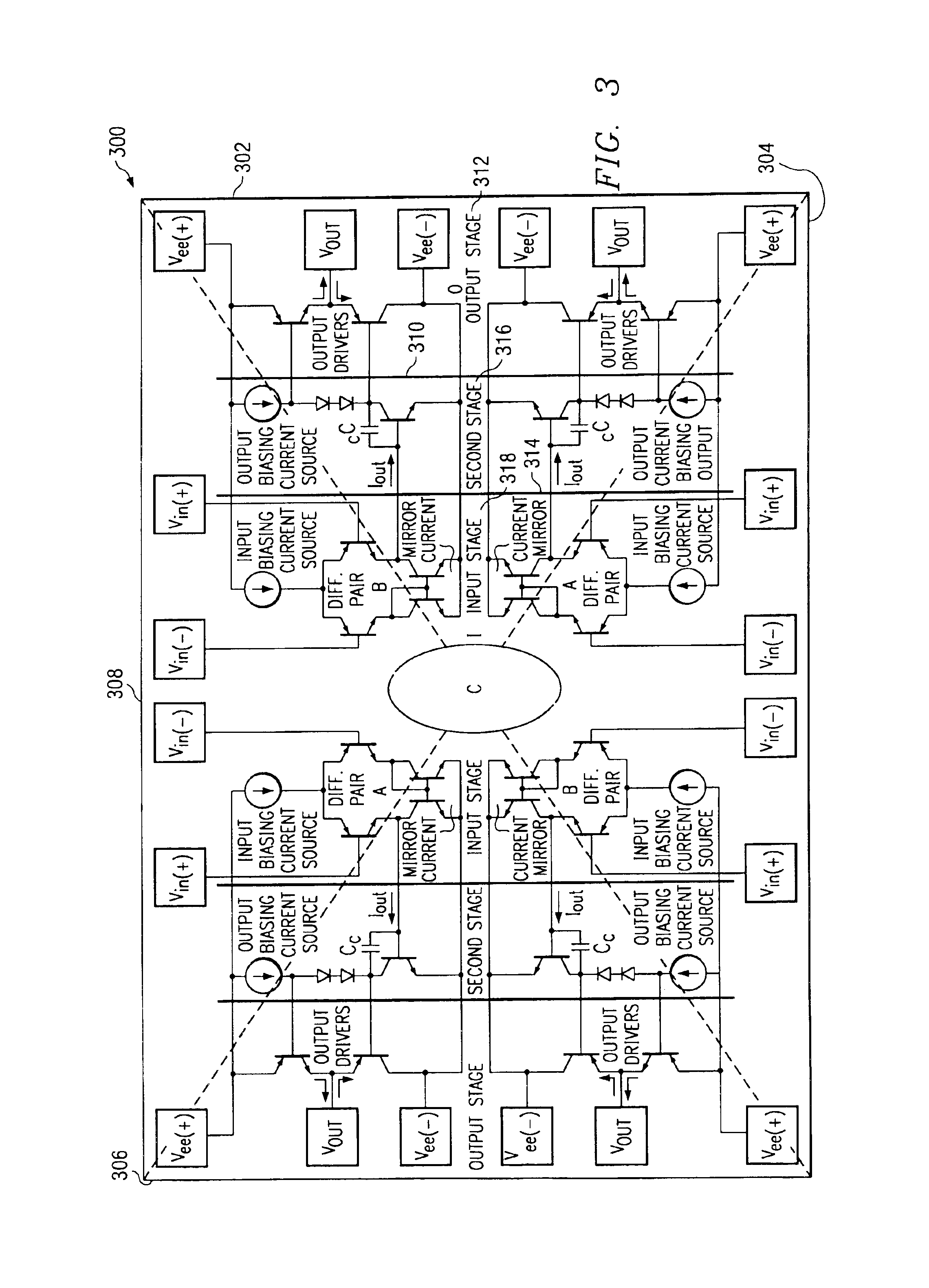
[0022]Reference throughout the specification to “one embodiment” means that a particular feature, structure, or characteristic described in connection with the embodiment is included in at least one embodiment of the present invention. Thus, the appearances of the phrases “in one embodiment” in various places throughout the specification are not necessarily all referring to the same embodiment. Furthermore, the particular features, structures, or characteristics may be combined in any suitable manner in one or more embodiments. Moreover, these embodiments are only examples of the many advantageous uses of the innovative teachings herein. In general, statements made in the specification of the present application do not necessarily limit any of the various claimed inventions. Moreover, some statements may apply to some inventive features, but not to others. In general, unless otherwise indicated, singular elements may be in the plural and vice versa with no loss of generality.

[0023]T...


PUM


Abstract

A method of reducing package stress includes placing matched components of an op-amp substantially in a region of a die having the least stress gradients. The region is located in the center of the die. Further, the center is the common centroid of the die. The matched components are the current mirror input stages of the op-amp. In one embodiment, a semiconductor configuration includes a die having a region with the least stress gradients, and an op-amp containing matched components that are located substantially in the region.

Description

FIELD OF THE INVENTION[0001]The present invention generally relates to reducing package stress and more particularly relates to operational amplifier (op-amp) layout techniques for reducing package stress.BACKGROUND OF THE INVENTION[0002]The performance characteristics of many linear and mixed signal integrated circuits are primarily dependent on the matching characteristics of current mirrors and differential amplifiers. In order to achieve a low offset voltage from an operational amplifier, the input transistors should be laid out identically. Otherwise, a DC offset may develop at the output of the circuit.[0003]In many op-amp applications, it is desirable to minimize the variance of the op-amp input offset voltage. Assembly induced package stress is the key factor behind many assembly and test (A / T) yield problems for operational amplifier devices. The primary component for the assembly induced shifts is mold compound. The contracting of the compound causes stress on the active c...

Claims


Application Information

Patent Timeline
Patent Type & Authority Patents(United States)
IPC IPC(8): H03F3/45H03F1/30H01L21/82H01L21/822H01L27/04
CPCH03F1/302H03F3/45085H03F3/45475H03F3/45
Inventor GRABHAM, MARTY A.CLINTON, BRIAN LANCE
Owner TEXAS INSTR INC
Why Eureka
Try Eureka