No-flow underfill process and material therefor

a flip chip and underfilling technology, applied in the direction of solid-state devices, basic electric elements, semiconductor devices, etc., can solve the problems of expensive process steps, complex process monitoring protocols, and high cost of process monitoring equipmen

Inactive Publication Date: 2005-09-13
INTEL CORP
View PDF23 Cites 24 Cited by
  • Summary
  • Abstract
  • Description
  • Claims
  • Application Information

AI Technical Summary

Benefits of technology

[0012]The present invention provides a no-flow underfill material and process suitable for underfilling flip chips and other bumped components employed in harsh environments. The underfill material and process are adapted to incorporate

Problems solved by technology

While highly-filled capillary-flow underfill materials have been widely and successfully used in flip chip assembly processes, expensive process steps are typically required to repeatably produce void-free underfills.
Capillary underfill materials require the use of expensive dispensing equipment, and the capillary underfill process is a batch-like process that disrupts an otherwise continuous flip chip assembly process.
Also, the adhesive strength of a capillary underfill material critically depends on the cleanliness of the die after reflow, necessitating costly cleaning equipment and complex process monitoring protocols.
These considerations limit the versatility of the flip chip underfill process to the extent that capillary underfilling is not practical for many flip chip

Method used


Image

  • No-flow underfill process and material therefor
  • No-flow underfill process and material therefor

Examples


Embodiment Construction

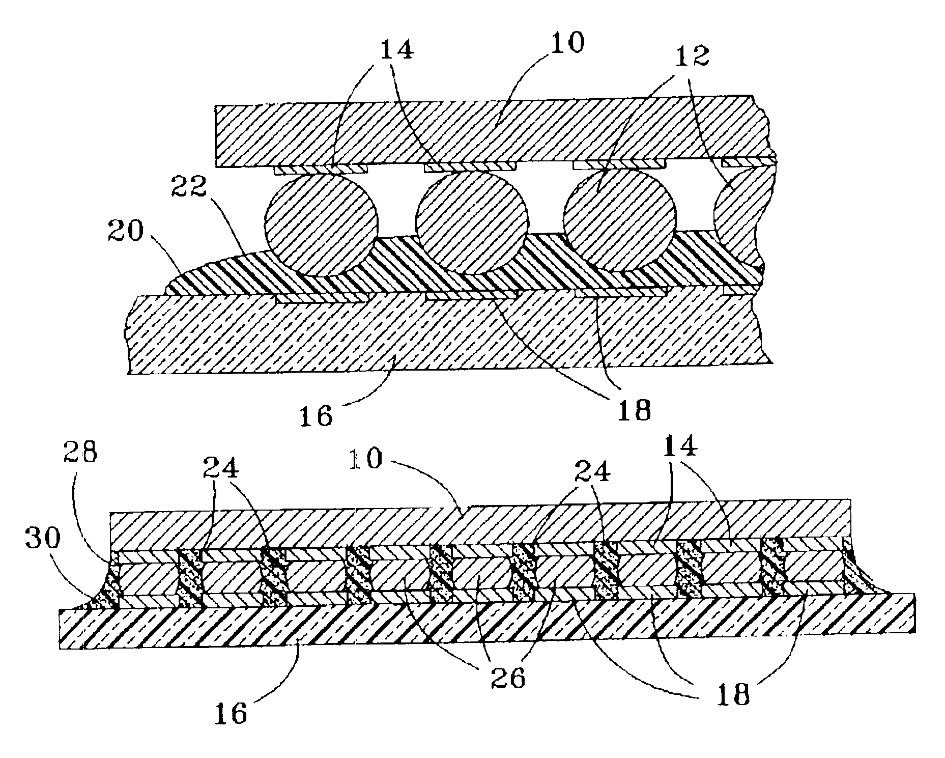
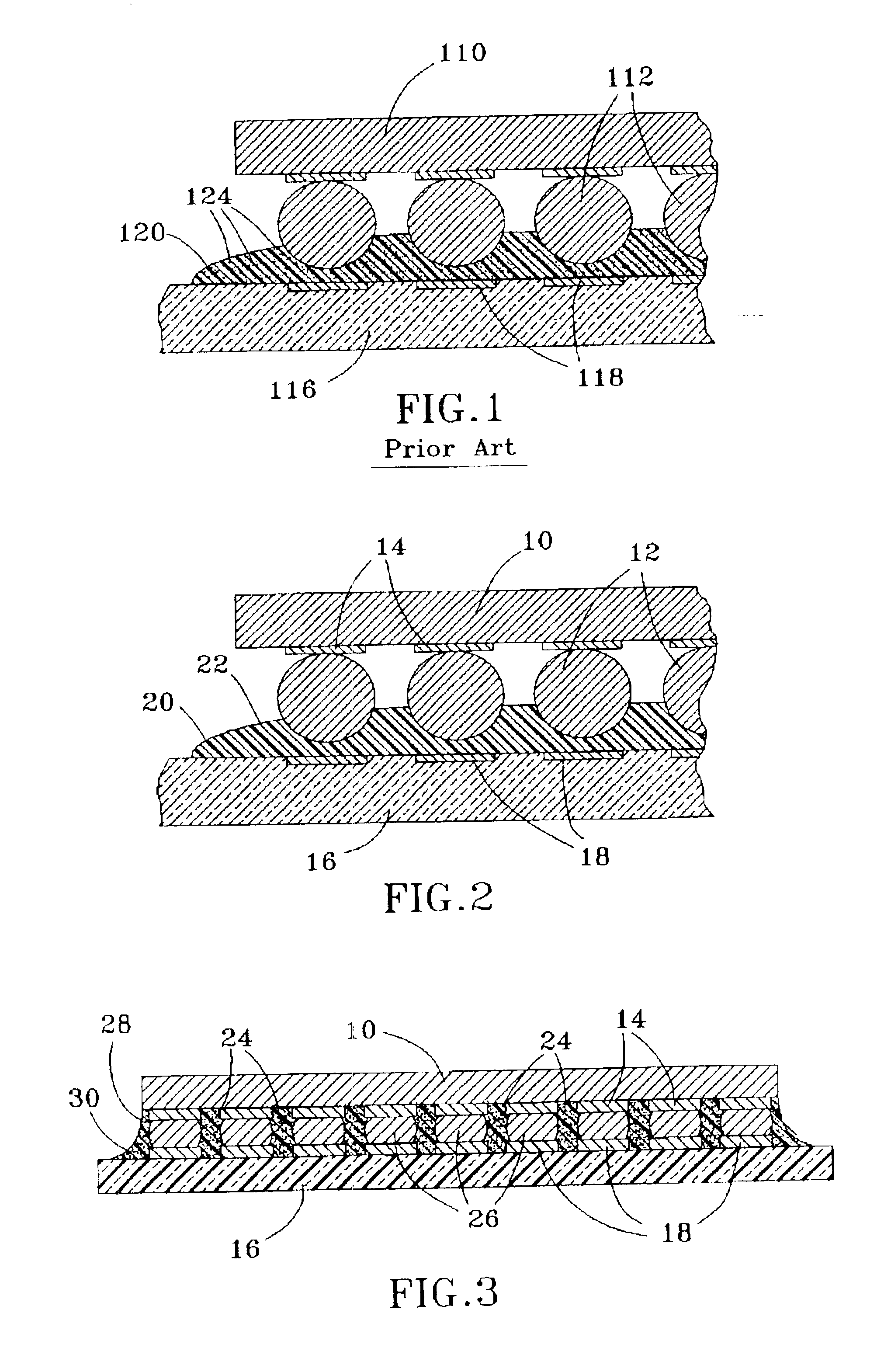
[0019]A no-flow underfill process in accordance with the present invention is schematically represented in FIGS. 2 and 3, by which a no-flow underfill material 20 is initially deposited in an unfilled condition (FIG. 2), but is formulated to form a particulate filler material 24 in situ (FIG. 3) following placement of a bumped circuit component 10. In FIG. 2, the underfill material 20 is shown as having been deposited on a substrate 16, which may be a circuit board formed of various materials, such as a thin organic laminate printed wiring board (PWB). As shown in FIG. 2, the circuit component, more specifically a flip chip die 10, is to be attached to the substrate 16 with solder bumps 12 formed on pads 14, such as under-bump metallurgy (UBM), defined on the die surface. The solder bumps 12 are intended to register with metal traces 18 (or other suitable terminals) on the substrate 16. While the underfill material 20 is represented as being deposited as a single layer, additional l...


PUM

PropertyMeasurementUnit
Dielectric polarization enthalpyaaaaaaaaaa
Flow rateaaaaaaaaaa
Adhesivityaaaaaaaaaa

Abstract

A no-flow underfill material and process suitable for underfilling a bumped circuit component. The underfill material initially comprises a dielectric polymer material in which is dispersed a precursor capable of reacting to form an inorganic filler. The underfill process generally entails dispensing the underfill material over terminals on a substrate, and then placing the component on the substrate so that the underfill material is penetrated by the bumps on the component and the bumps contact the terminals on the substrate. The bumps are then reflowed to form solid electrical interconnects that are encapsulated by the resulting underfill layer. The precursor may be reacted to form the inorganic filler either during or after reflow.

Description

CROSS REFERENCE TO RELATED APPLICATIONS[0001]Not applicable.STATEMENT REGARDING FEDERALLY SPONSORED RESEARCH[0002]Not applicable.BACKGROUND OF THE INVENTION[0003](1) Field of the Invention[0004]The present invention generally relates to underfill materials for flip chip devices. More particularly, this invention relates to a no-flow material for underfilling a flip chip device and an underfill method using the no-flow material.[0005](2) Description of the Related Art[0006]Underfilling is well known for promoting the reliability of flip chip components, such as flip chips and ball grid array (BGA) packages that are physically and electrically connected to traces on organic or inorganic circuit boards with numerous solder bump connections. A basic function of an underfill material is to reduce the thermal expansion mismatch loading on the solder joints that electrically and physically attach a component, e.g., die, to an inorganic or organic substrate, such as a reinforced epoxy resin...

Claims


Application Information

Patent Timeline
IPC IPC(8): H01L21/56H01L21/02H01L23/28H01L23/29C08K5/00C08K5/54H01L21/60
CPCH01L21/563H01L23/293H01L24/81H01L24/29C08K5/54H01L2224/16225H01L2224/73204H01L2224/81801H01L2224/83192H01L2924/01033H01L2924/0105H01L2924/01075H01L2924/01082H01L2924/01322H01L2924/01006H01L2924/014H01L2924/3512H01L2924/00H01L2224/81191H01L2224/131H01L24/05H01L2224/05568H01L2224/05573H01L2224/056H01L2924/12042H01L2924/00014
Inventor CHAUDHURI, ARUN K.WORKMAN, DEREK B.STEPNIAK, FRANKWALSH, MATTHEW R.
Owner INTEL CORP
Why Eureka
Try Eureka