Flip chip mounting method of forming a solder bump on a chip pad that is exposed through an opening formed in a polyimide film that includes utilizing underfill to bond the chip to a substrate

Active Publication Date: 2005-09-13
RENESAS ELECTRONICS CORP
View PDF5 Cites 9 Cited by
  • Summary
  • Abstract
  • Description
  • Claims
  • Application Information

AI Technical Summary

Benefits of technology

[0011]An object of the present invention is to provide a flip chip mounting method by which a semiconductor chip and an assembly substrate are not readily stripped from each other in the case where the semiconductor chip and assembly substrate are bonded by a flip chip method using an underfill resin.
[0013]When removing the insulation film, a reaction product of the insulation film does not adhere to the surface of the polyimide film. Therefore, reduction in adhesion of the semiconductor chip and assembly substrate to the underfill resin due to the reaction product can be prevented, allowing adhesion between the chip and assembly substrate to be promoted.

Problems solved by technology

In the case where the semiconductor chip and assembly substrate are bonded by flip chip mounting using an underfill resin with the cured layer formed on the polyimide film, adhesion between the underfill resin and cured layer is poor, which problematically causes the assembly substrate and semiconductor chip to be stripped from each other during device operation.
Poor adhesion between the assembly substrate and semiconductor chip had not been in question with semiconductor chips having smaller area, but has become perceived as a problem with a recent trend toward larger area of semiconductor chips.

Method used


Image

  • Flip chip mounting method of forming a solder bump on a chip pad that is exposed through an opening formed in a polyimide film that includes utilizing underfill to bond the chip to a substrate
  • Flip chip mounting method of forming a solder bump on a chip pad that is exposed through an opening formed in a polyimide film that includes utilizing underfill to bond the chip to a substrate
  • Flip chip mounting method of forming a solder bump on a chip pad that is exposed through an opening formed in a polyimide film that includes utilizing underfill to bond the chip to a substrate

Examples


first preferred embodiment

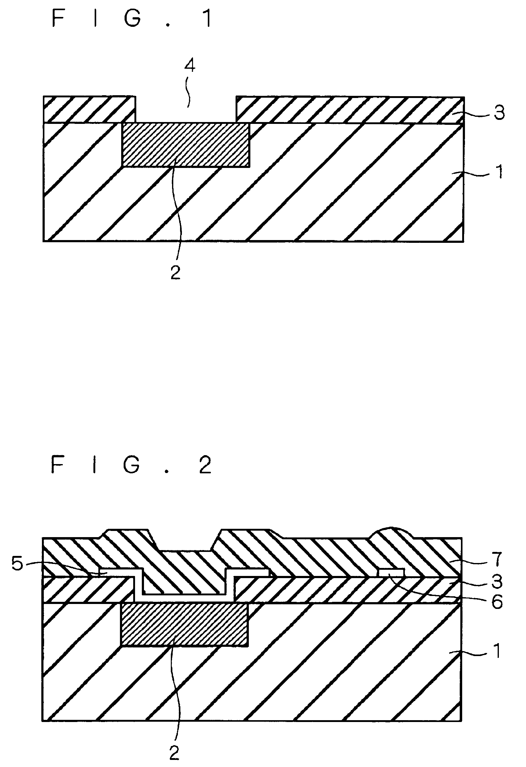
[0025]A first preferred embodiment is directed to the case of using a single-layer passivation film. A flip chip mounting method according to the present embodiment will specifically be described referring to sectional views showing manufacturing steps.

[0026]FIG. 1 illustrates part of the surface of a semiconductor chip before or after being separated from a wafer. As shown, a copper interconnect line 2 is provided in the surface of an interlayer insulation film 1, and an insulation film 3 is formed to cover the interlayer insulation film 1 and copper interconnect line 2. Next, part of the insulation film 3 covering the copper interconnect line 2 is removed to form a recess 4 in the surface of the insulation film 3, so that the copper interconnect line 2 is exposed from the bottom of the recess 4.

[0027]Next, as shown in FIG. 2, a pad 5 made of aluminum or the like is formed to cover the bottom and side surfaces of the recess 4 and part of the upper surface of the insulation film 3 n...

second preferred embodiment

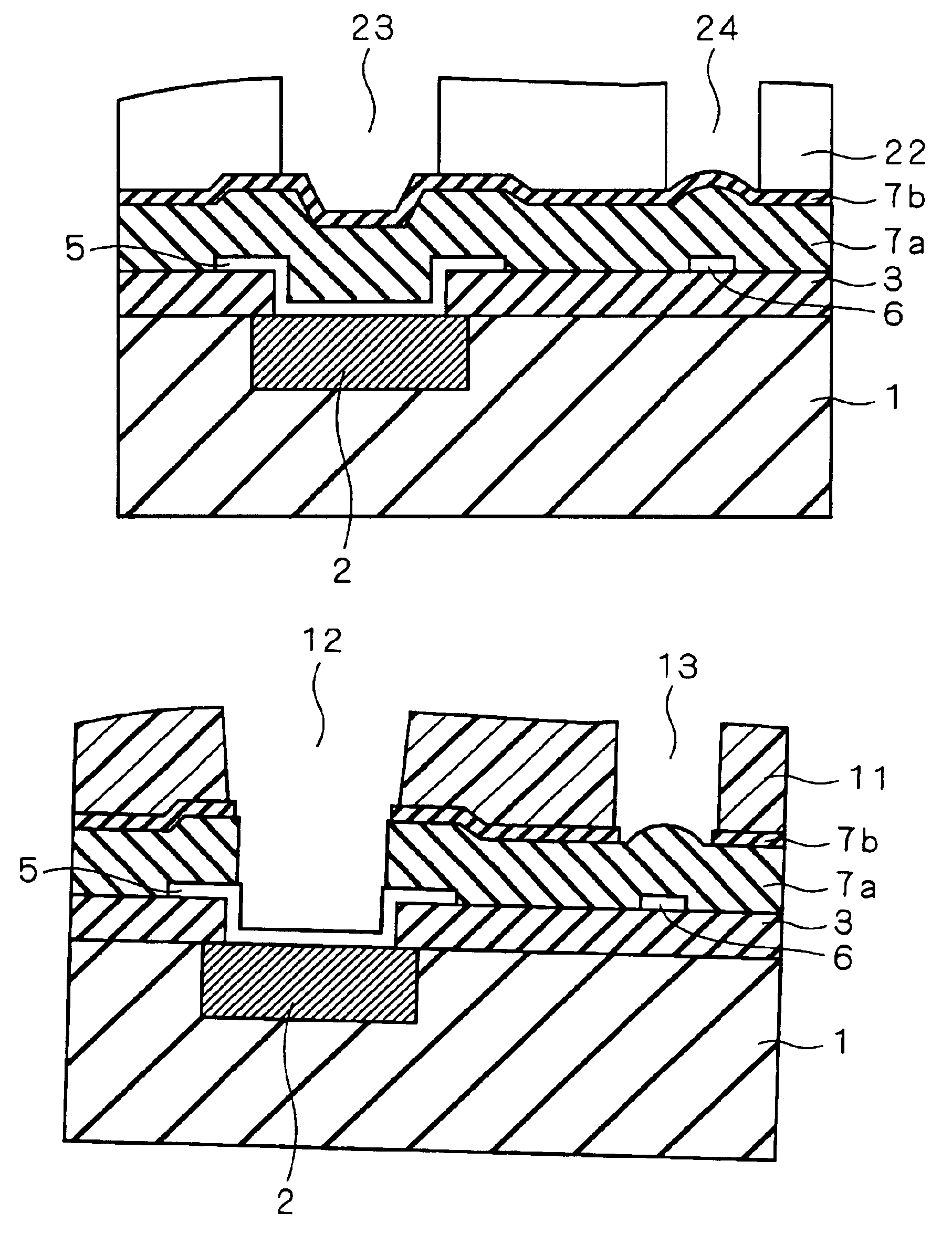
[0042]A second preferred embodiment is directed to the case of using a two-layered passivation film (in which a nitride film and an oxide film are stacked). A flip chip mounting method according to the present embodiment will specifically be described referring to sectional views showing manufacturing steps. The steps are the same as those in the first preferred embodiment as far as the structure shown in FIG. 2 is obtained, repeated explanation of which is thus omitted here. In the present embodiment, the first layer of the passivation film is a silicon oxide film 7a.

[0043]Next, as shown in FIG. 12, a silicon nitride film 7b is formed as the second layer of the passivation film by the CVD method or the like to cover the silicon oxide film 7a. Here, the silicon nitride film 7b functions as moisture barrier for the copper interconnect line 2 and the like.

[0044]Next, as shown in FIG. 13, a resist 22 is coated to cover the silicon nitride film 7b, and exposure and development is perfo...

third preferred embodiment

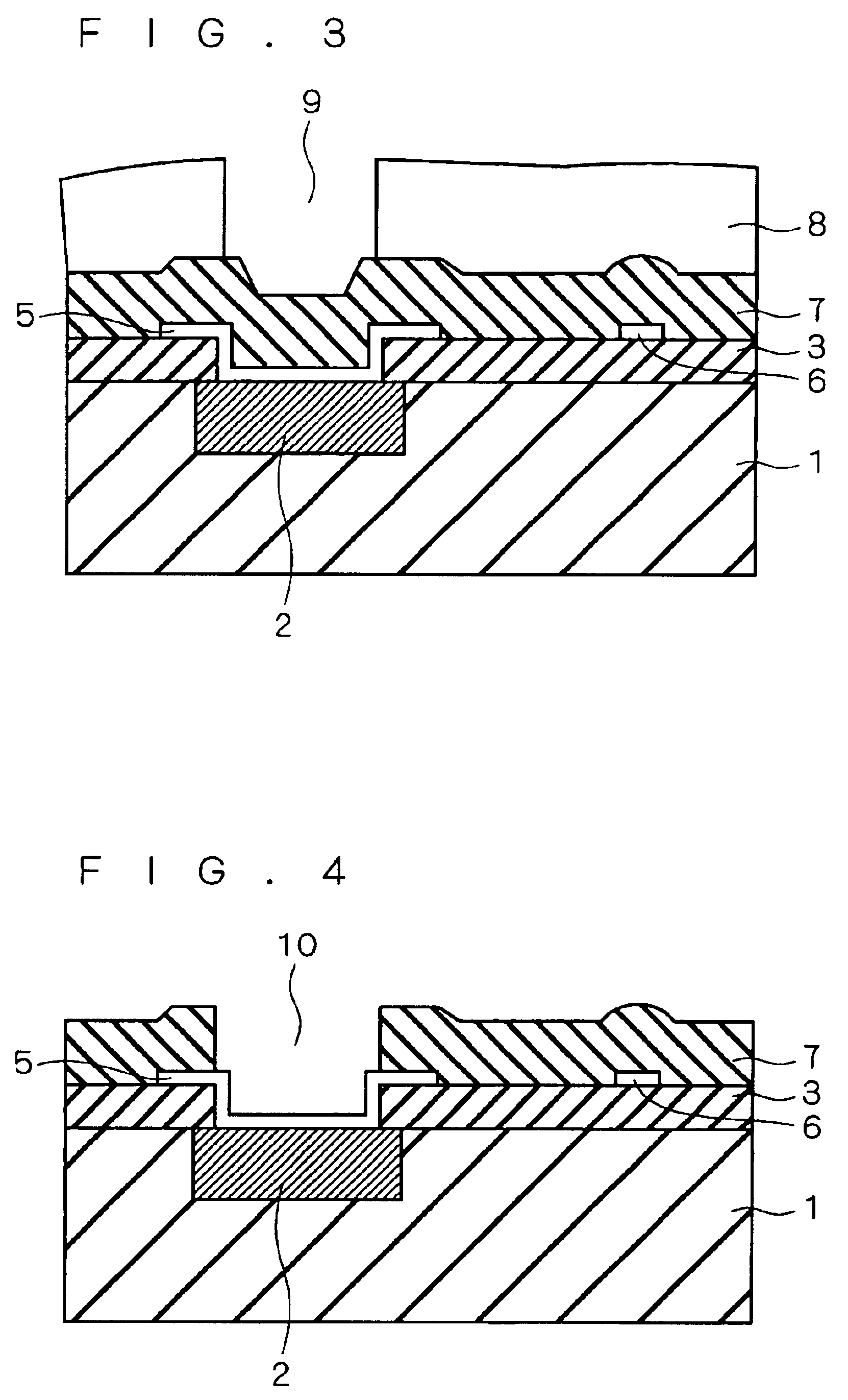
[0051]A third preferred embodiment is also directed to the case of using a two-layered passivation film (in which a nitride film and an oxide film are stacked), however, the passivation film is removed with different steps from those in the second preferred embodiment. A flip chip mounting method according to the present embodiment will specifically be described referring to sectional views showing manufacturing steps.

[0052]First, a semiconductor chip having the structure as described in the first preferred embodiment as shown in FIG. 2 is formed, and the silicon nitride film 7b is formed over the silicon oxide film 7a as described in the second preferred embodiment referring to FIG. 12.

[0053]Next, as shown in FIG. 18, a resist 31 is coated to cover the silicon nitride film 7b, and exposure and development is performed to form an opening 32 in the surface of the resist 31 above the pad 5. The silicon nitride film 7b is exposed from the bottom surface of the opening 32.

[0054]Next, an...


PUM


Abstract

A semiconductor chip (15) having a pad (5) covered with a passivation film (7) is prepared, and the passivation film (7) over the pad (5) is selectively removed to expose the pad (5). Next, a polyimide film (11) having an opening (12) for exposing the pad (5) is formed on the passivation film (7). Thereafter, solder bumps (14) are formed on the pad (5), and an underfill resin (17) is filled between an assembly substrate (16) and the semiconductor chip (15) to bond the assembly substrate (16) and semiconductor chip (15) with the solder bumps (14) interposed therebetween.

Description

BACKGROUND OF THE INVENTION[0001]1. Field of the Invention[0002]The present invention relates to a flip chip mounting method, and more particularly to a method of manufacturing a flip chip prior to being mounted.[0003]2. Description of the Background Art[0004]With a flip chip mounting method for bonding a semiconductor chip and an assembly substrate with solder bumps interposed therebetween, stress concentrates on the solder bumps with thermal change and impact occurring after bonding, causing the solder bumps to be stripped from the semiconductor chip or assembly substrate.[0005]Thus, a method has been employed by which an underfill resin is filled between a semiconductor chip and an assembly substrate in order to ease concentration of stress on solder bumps and to promote adhesion between the semiconductor chip and assembly substrate (e.g., Japanese Patent Application Laid-Open No. 2002-203866; FIG. 1).[0006]For flip chip mounting, a pad covered with a passivation film needs to be...

Claims


Application Information

Patent Timeline
IPC IPC(8): H01L23/525H01L21/56H01L21/02H01L21/60H01L23/48H01L23/52H01L23/28H01L23/29H01L23/485
CPCH01L21/563H01L23/296H01L23/5256H01L24/11H01L24/28H01L24/81H01L24/13H01L2224/1147H01L2224/13099H01L2224/16225H01L2224/73203H01L2224/73204H01L2224/81801H01L2224/83102H01L2224/92125H01L2924/01004H01L2924/01005H01L2924/01013H01L2924/01029H01L2924/01078H01L2924/01082H01L2924/01006H01L2924/01033H01L2924/014H01L2224/131H01L2924/0001H01L2224/05001H01L2224/05022H01L2224/05572H01L2224/05624H01L2924/00014H01L2224/05147
Inventor MAEDA, HIROSHI
Owner RENESAS ELECTRONICS CORP
Why Eureka
Try Eureka