Method and apparatus for providing an integrated membrane switch and capacitive sensor

a capacitive sensor and membrane switch technology, applied in the field of capacitive touch pad sensors, can solve the problems of false reading of touch, inconvenient use, and damage to conductive elements, and achieve the effect of stiffening the circuit assembly

Inactive Publication Date: 2005-09-13
SYNAPTICS INC
View PDF26 Cites 150 Cited by
  • Summary
  • Abstract
  • Description
  • Claims
  • Application Information

AI Technical Summary

Benefits of technology

[0017]This invention incorporates a membrane switch keystroke sensing element of a keyboard device and a sensing element of a capacitive touch pad device onto one circuit assembly. The circuit assembly has a preventative capacitance configuration that limits non-intentional capacitive couplings that may give false readings in a capacitive touch pad sensor. This allows a producer of such devices to take advantage of economies of scale, to reduce the amount of material, time, knowledge base, and equipment needed to produce sensor circuit assemblies, to simplify installation of circuit assembly into a base and to reduce component count.

Problems solved by technology

One problem with resistive touch pad sensors is that the conductive elements are susceptible to damage and wear.
Any warping of the conductive elements from bending, breaking, or misalignment may cause the conductive elements to contact and lead to false readings of touch.
However, incorporating resistive touch pad membrane switch sensors and membrane switch keystroke sensors yield non-optimal solutions since resistive sensors often require more costly and significantly different manufacturing and assembly processes then membrane switch keystroke sensors.

Method used


Image

  • Method and apparatus for providing an integrated membrane switch and capacitive sensor
  • Method and apparatus for providing an integrated membrane switch and capacitive sensor
  • Method and apparatus for providing an integrated membrane switch and capacitive sensor

Examples


second embodiment

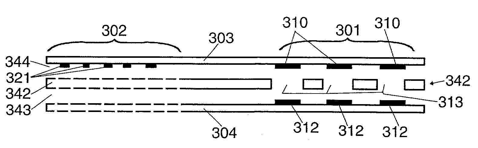
[0081]FIG. 7 illustrates a cross sectional view along line 199 of circuit assembly 300 having two layers of conductive material in capacitive sensor area 302. In FIG. 7, electrodes 323 are in a third pattern 344 of conductive material. Third pattern 344 is in a plane that is substantially parallel to first pattern 341, second pattern 343, and insulating member 342. In FIG. 7, third pattern 344 is affixed to a top side of substrate 303 that is opposite of the side of substrate 303 to which first pattern 341 is affixed. The other components of circuit assembly 300 shown in FIG. 7 are configured as described with reference to FIG. 6.

third embodiment

[0082]FIG. 8 illustrates a cross sectional view along line 199 of circuit assembly 300 having two layers of conductive material in capacitive sensor area 302. In FIG. 8, electrodes 323 are in a third pattern 344 of conductive material. Third pattern 344 is in a plane that is substantially parallel to first pattern 341, second pattern 343, and insulating member 342. In FIG. 8, third pattern 344 is affixed to inner surface of textured material 1001. The other components of circuit assembly 300 shown in FIG. 8 are configured as described with reference to FIG. 6.

fourth embodiment

[0083]FIG. 9 illustrates a cross sectional view along line 199 of circuit assembly 300 having two layers of conductive material in capacitive sensor area 302. In FIG. 9, electrodes 323 are in a third pattern 344 of conductive material. Third pattern 344 is in a plane that is substantially parallel to first pattern 341, second pattern 343, and insulating member 342. Third pattern 344 is affixed to a top side of a rigid substrate 398. Rigid substrate 398 is a printed circuit board in an exemplary embodiment. The other components of circuit assembly 300 shown in FIG. 9 are configured as described with reference to FIG. 6.

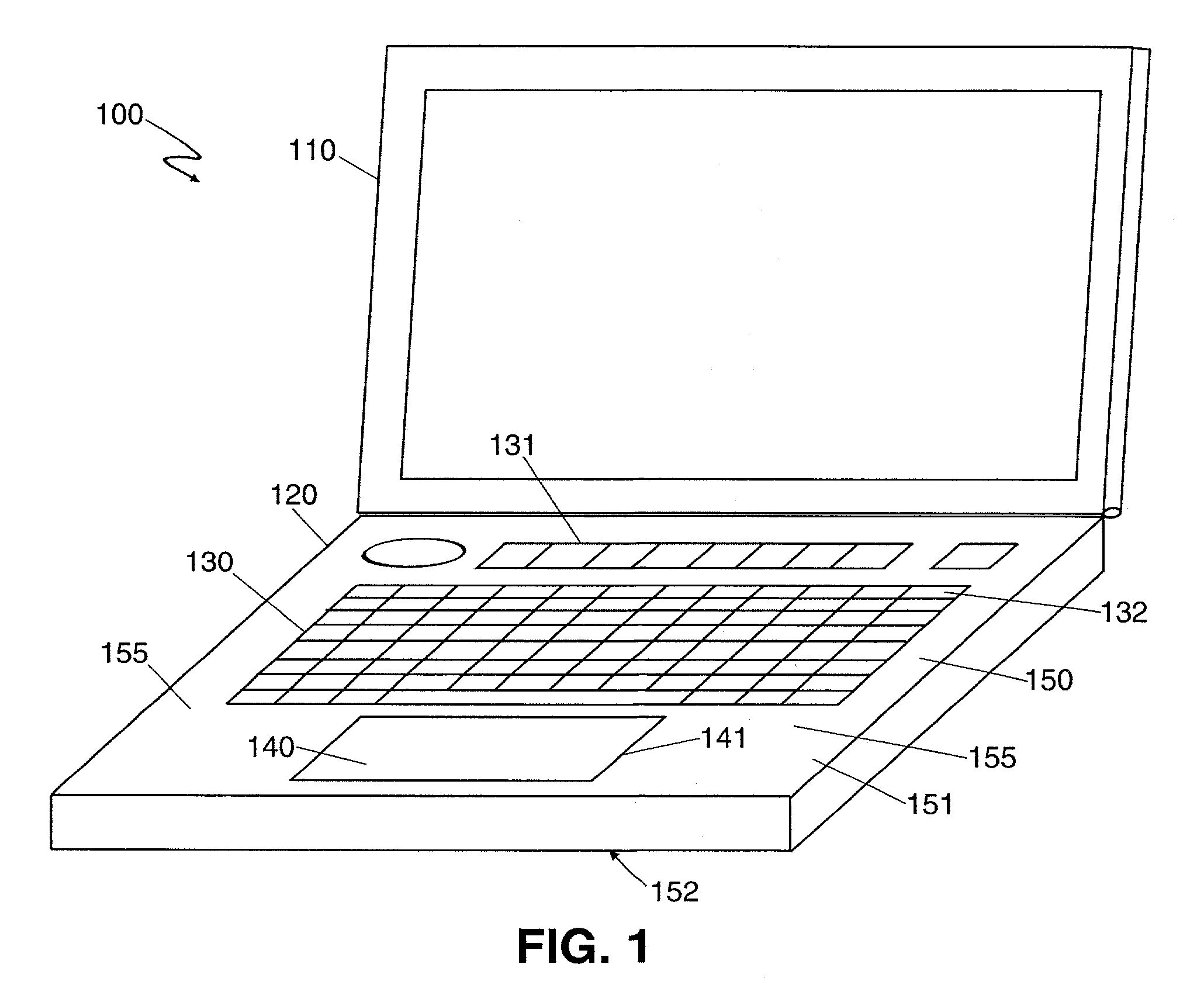
[0084]FIG. 10 illustrates an exploded view of an exemplary sensor circuit assembly 300 for use in notebook computer system 100 (shown in FIG. 1) in accordance with this invention. One skilled in the art will recognize that this is a non-limiting example used to point out the features and advantages of this invention. Circuit assembly 300 has a membrane switch sensor ar...


PUM


Abstract

A circuit assembly for providing a switch sensor and a capacitive sensor. The circuit assembly has a first pattern of conductive material in a first plane and a second pattern of conductive material in a second plane. An insulating member in an intermediate plane separates the first and second patterns. In a switch sensor area, the insulating member has openings to allow a first conductive element in the first pattern to contact a second conductive element in the second pattern responsive a force being applied to the first conductive element. In the capacitive sensor area, the insulating member maintains spacing between conductive material in the first and second patterns. The circuit assembly also includes a preventative capacitance configuration that limits non-intentional capacitive coupling in the capacitive sensor area.

Description

CROSS-RELATED[0001]This application is a utility application claiming priority to an earlier filed U.S. Provisional Application No. 60 / 377,932 filed May 3, 2002.FIELD OF THE INVENTION[0002]This invention relates to capacitive touch pad sensors. More particularly, this invention relates to incorporating a capacitive touch pad sensor into a membrane switch sensor. Still more particularly, this invention relates to a capacitive touch pad sensor produced on a circuit assembly of a membrane switch sensor while reducing non-intentional capacitive coupling in the capacitive touch pad sensor.STATEMENT OF THE PRIOR ART[0003]In today's society, many types of systems require two or more input devices to receive inputs from a user. A good example is a personal computer system. In a personal computer system, a keyboard device receives keystroke information from a user to receive alphanumeric inputs and a mouse or other analog pointing device receives cursor control inputs. Other examples of syst...

Claims


Application Information

Patent Timeline
Patent Type & Authority Patents(United States)
IPC IPC(8): H03M11/00
CPCG06F3/044H01H2239/006H03K17/962H03K2217/94015H03K2217/960765G06F3/0445
Inventor BOLENDER, ROBERT JAMESCHENG, WENDY H. W.
Owner SYNAPTICS INC
Why Eureka
Try Eureka