Non-volatile semiconductor memory with large erase blocks storing cycle counts

a non-volatile semiconductor and erase block technology, applied in the field of non-volatile semiconductor memories, can solve problems such as adversely affecting the decision-making of memory controllers

Inactive Publication Date: 2005-09-13
KIOXIA CORP +1
View PDF53 Cites 91 Cited by
  • Summary
  • Abstract
  • Description
  • Claims
  • Application Information

AI Technical Summary

Benefits of technology

[0017]As is a trend to increase the amount of data that a given number of memory cells can store, more than one bit of user data is preferably stored in each memory cell storage element by establishing more than two programmed states for each storage element. For the block cycle count data, however, there are advantages to storing that data in two states, or one bit per memory cell storage element. The cycle count data programming is improved and this programming may be done in a manner that reduces the amount of disturbs of the newly erased block into which it is written.

Problems solved by technology

When invalid, the block is mapped out of the system because the number of erase cycles that it has experienced is unknown, and this uncertainty can adversely affect decisions that are made by the memory controller in operation of the block.

Method used


Image

  • Non-volatile semiconductor memory with large erase blocks storing cycle counts
  • Non-volatile semiconductor memory with large erase blocks storing cycle counts
  • Non-volatile semiconductor memory with large erase blocks storing cycle counts

Examples


Embodiment Construction

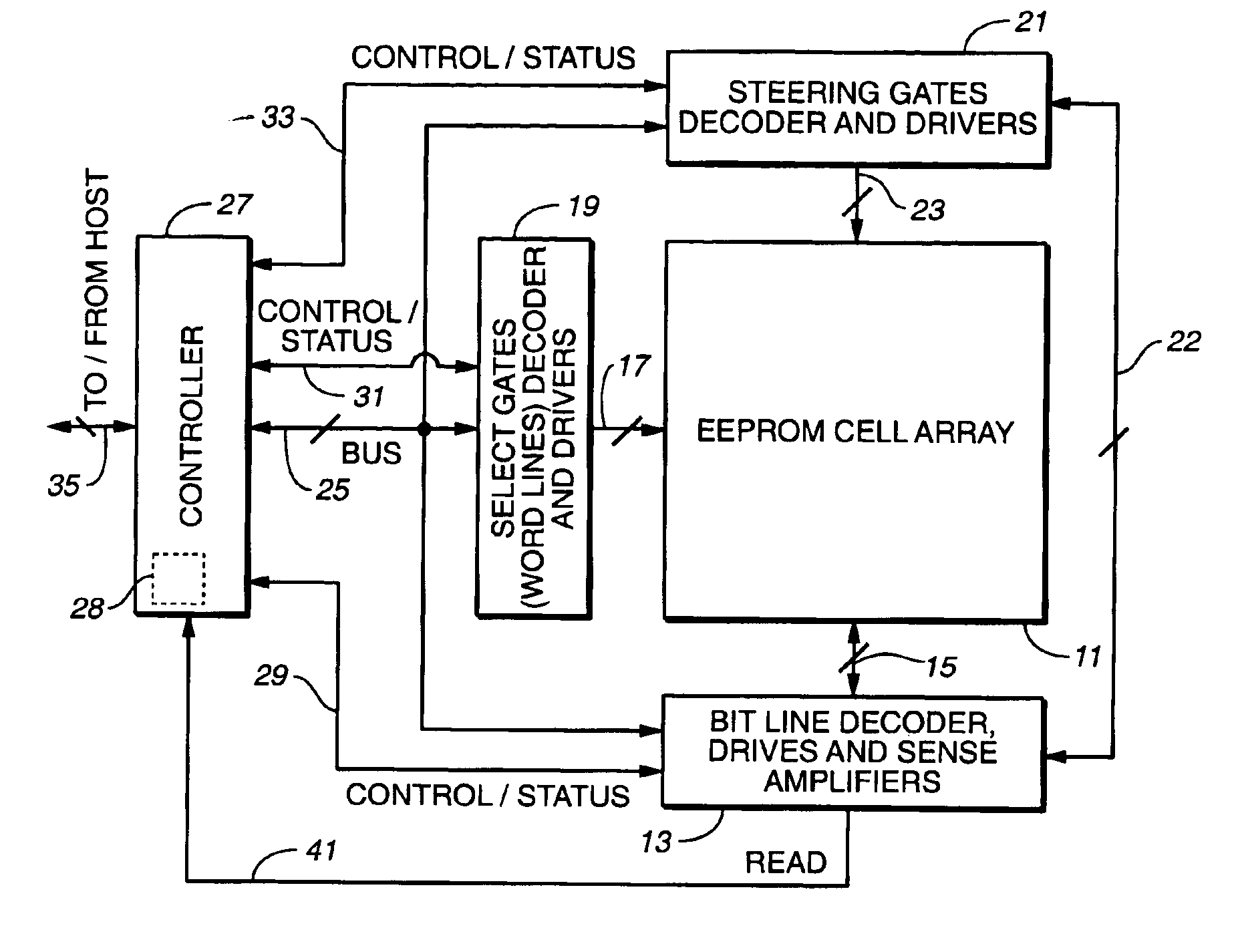
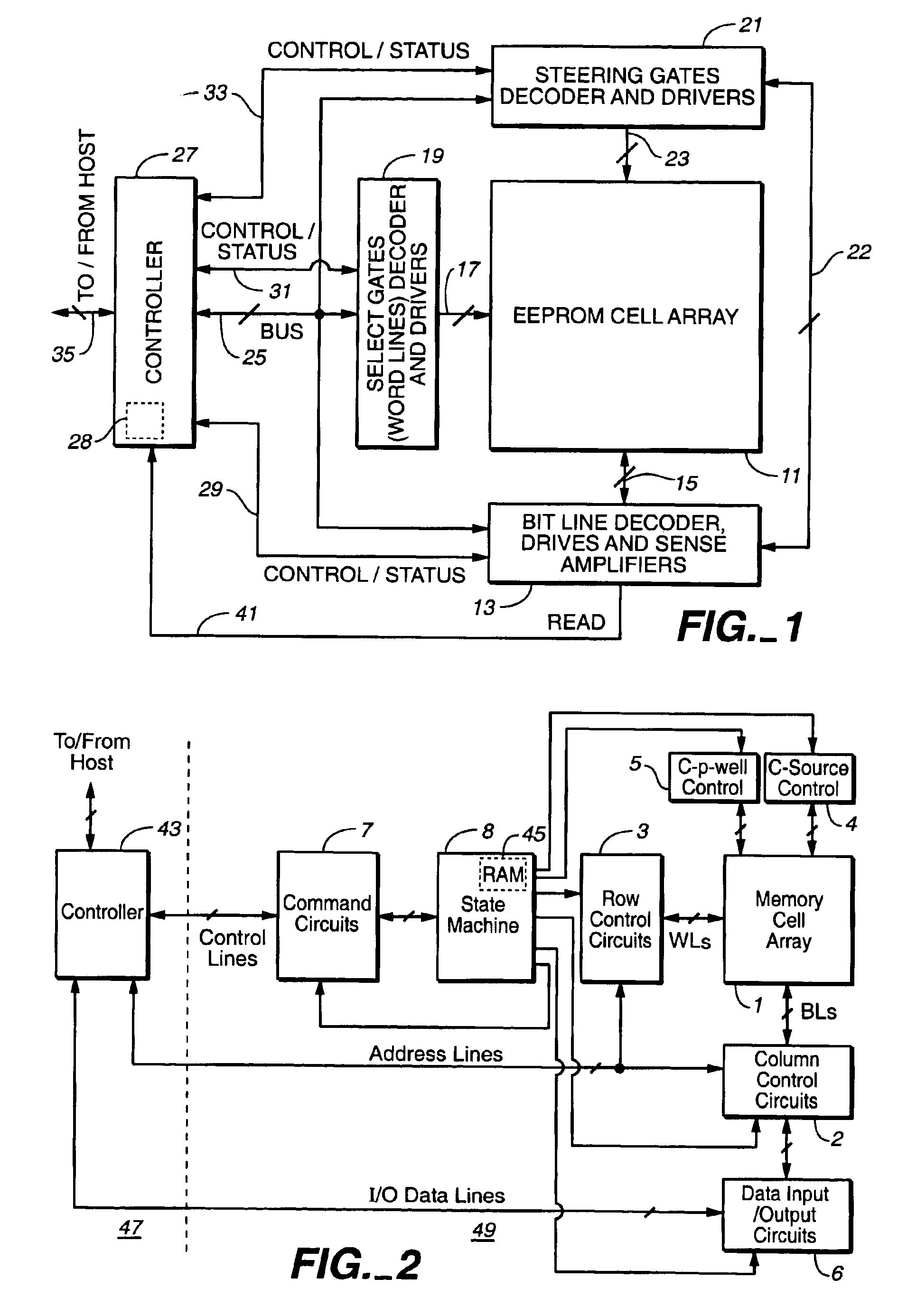
[0030]An example memory system in which the various aspects of the present invention may be implemented is illustrated by the block diagram of FIG. 1. A large number of individually addressable memory cells 11 are arranged in a regular array of rows and columns, although other physical arrangements of cells are certainly possible. This system is particularly adapted for the array 11 to be the NOR type, as described above in the Background and in references incorporated herein. Bit lines, designated herein to extend along columns of the array 11 of cells, are electrically connected with a bit line decoder and driver circuit 13 through lines 15. Word lines, which are designated in this description to extend along rows of the array 11 of cells, are electrically connected through lines 17 to a word line decoder and driver circuit 19. Steering gates, which extend along columns of memory cells in the array 11, are electrically connected to a steering gate decoder and driver circuit 21 thr...


PUM


Abstract

In a flash EEPROM system that is divided into separately erasable blocks of memory cells with multiple pages of user data being stored in each block, a count of the number of erase cycles that each block has endured is stored in one location within the block, such as in spare cells of only one page or distributed among header regions of multiple pages. The page or pages containing the block cycle count are initially read from each block that is being erased, the cycle count temporarily stored, the block erased and an updated cycle count is then written back into the block location. User data is then programmed into individual pages of the block as necessary. The user data is preferably stored in more than two states per memory cell storage element, in which case the cycle count can be stored in binary in a manner to speed up the erase process and reduce disturbing effects on the erased state that writing the updated cycle count can cause. An error correction code calculated from the cycle count may be stored with it, thereby allowing validation of the stored cycle count.

Description

FIELD OF THE INVENTION[0001]This invention relates generally to non-volatile semiconductor memories and their operation, particularly to the use of memory cell block erase / write cycle counts.BACKGROUND[0002]There are many commercially successful non-volatile memory products being used today, particularly in the form of small form factor cards, which use an array of flash EEPROM (Electrically Erasable and Programmable Read Only Memory) cells.NOR Array[0003]In a typical NOR array, memory cells are connected between adjacent bit line source and drain diffusions that extend in a column direction with control gates connected to word lines extending along rows of cells. One typical memory cell has a “split-channel” between source and drain diffusions. A charge storage element of the cell is positioned over one portion of the channel and the word line (also referred to as a control gate) is positioned over the other channel portion as well as over the charge storage element. This effective...

Claims


Application Information

Patent Timeline
Patent Type & Authority Patents(United States)
IPC IPC(8): G06F12/00G11C16/34G11C11/21G11C11/24G11C11/34G11C16/04G11C16/06G11C11/56H01L27/115
CPCG06F11/1068G11C11/5621G11C11/5635G11C16/0483G11C16/3459G11C16/349G11C16/3427G11C2211/5646G11C2211/5641
Inventor CHEN, JIANTANAKA, TOMOHARU
Owner KIOXIA CORP
Why Eureka
Try Eureka