

CMOS receiver for simultaneous bi-directional links
a receiver and simultaneous bi-directional technology, applied in the field ofdifferential receiver circuits, can solve the problems of faulty switching at the receiving end, limited noise tolerance, and electrical noise induced on one line is also induced on the other
- Summary
- Abstract
- Description
- Claims
- Application Information
AI Technical Summary
Benefits of technology
Problems solved by technology
Method used
Image

Examples
Embodiment Construction
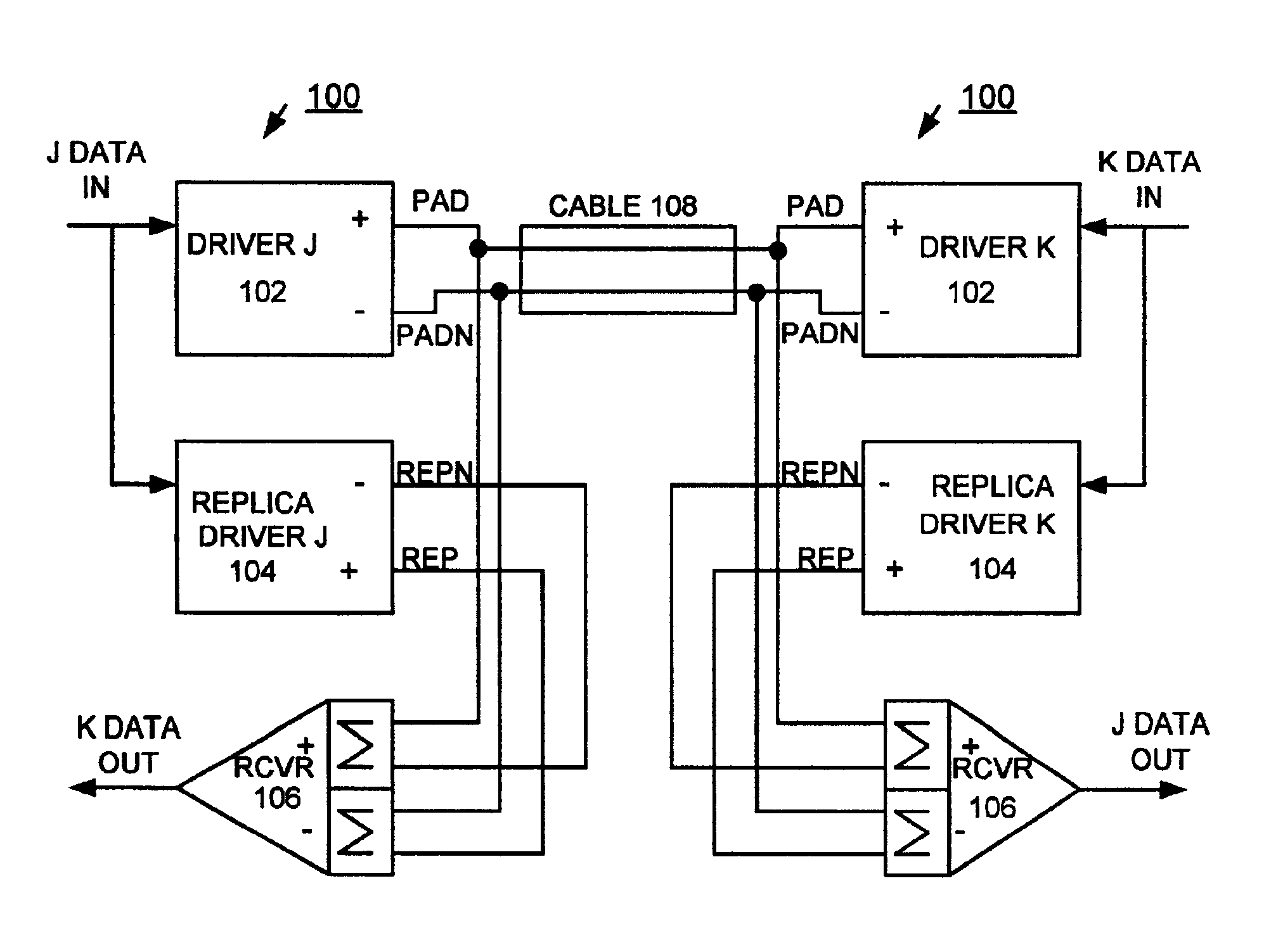
[0019]Having reference now to the figures, and in particular FIG. 1, there is shown a CMOS bi-directional current mode differential link generally designated by the reference character 100. The CMOS bi-directional current mode differential link 100 includes a driver 102 and a replica driver 104. Driver 102 and replica driver 104 are coupled to a receiver 106. As shown in FIG. 1, a differential wire pair 108 couples two CMOS bi-directional current mode differential links 100. Such a differential wire pair 108 is also known as a transmission line. CMOS bi-directional current mode differential link 100 provides for simultaneous bi-directional signaling over the differential wire pair. “J DATA IN” is data to be driven from the left instance of link 100 to the right instance of link 100, to be received as “J DATA OUT”. “K DATA IN” is data to be driven from the right instance of link 100 to the left instance of link 100, to be received as “K DATA OUT”.
[0020]U.S. Pat. No. 6,304,106 B1, alr...
PUM
 Abstract
Description
Claims
Application Information