Process for electroplating metal into microscopic recessed features

a technology of recessed features and electrochemical deposition, which is applied in the direction of superimposed coating process, printed element electric connection formation, coating, etc., can solve the problems of poor electroplating, poor electrical quality of feature sidewalls and bottoms, and increased difficulty in electroplating without seams and/or voids, etc., to achieve fast plating rate, increase the aspect ratio, and reduce the effect of surface reaction resistan

Inactive Publication Date: 2005-09-20
NOVELLUS SYSTEMS
View PDF15 Cites 67 Cited by
  • Summary
  • Abstract
  • Description
  • Claims
  • Application Information

AI Technical Summary

Benefits of technology

[0063]FIGS. 39 and 40 show the effect of conformally depositing another layer (“backfilled”), amorphous silicon in these figures to increase the aspect ratio. This is a technique to study the electroplating of smaller features when such features may not be reliably fabricated by present technology. Different magnifications are shown.
[0064]FIG. 41 shows the initiation phase plating (phase 2) using low currents such that the relative resistance of feature top and bottom is high in comparison with diffusion resistance. At low current, the relative resistance of surface reaction to diffusion is high. Thus, conformal plating occurs without substantial depletion effect (depletion of copper due to reaction occurring faster than diffusion to the reaction site). Slow plating rate favors conformal plating. Additionally, low plating current has a small additive depletion effect, further increasing conformality. Bottom-up filling does not occur at these low current levels, 0.5 amp.

Problems solved by technology

However, as integrated circuit features become ever smaller, electroplating without the formation of seams and / or voids becomes more challenging.
Deposit of a conducting seed layer onto a substrate and microscopic recessed features often does not provide adequate metallization of the feature walls, leading to poor electroplating.
The poor electrical quality of feature sidewalls and bottom is observed to worsen when the substrate is brought into contact with the electroplating solution.

Method used


Image

  • Process for electroplating metal into microscopic recessed features
  • Process for electroplating metal into microscopic recessed features
  • Process for electroplating metal into microscopic recessed features

Examples


Embodiment Construction

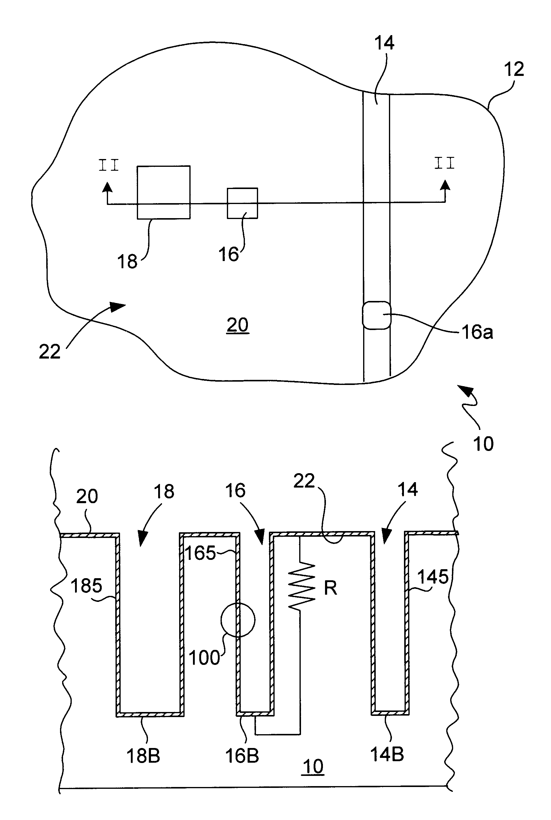
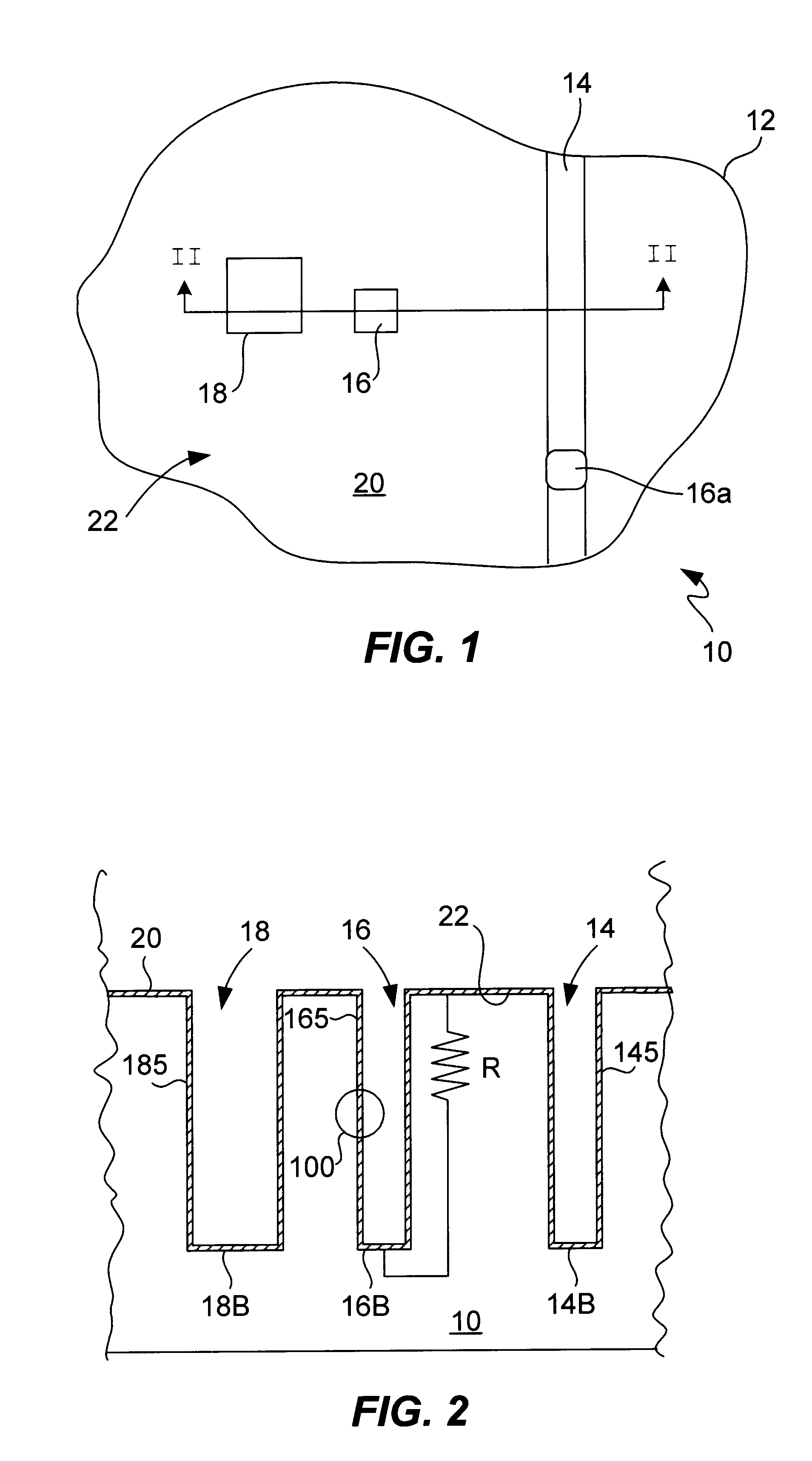
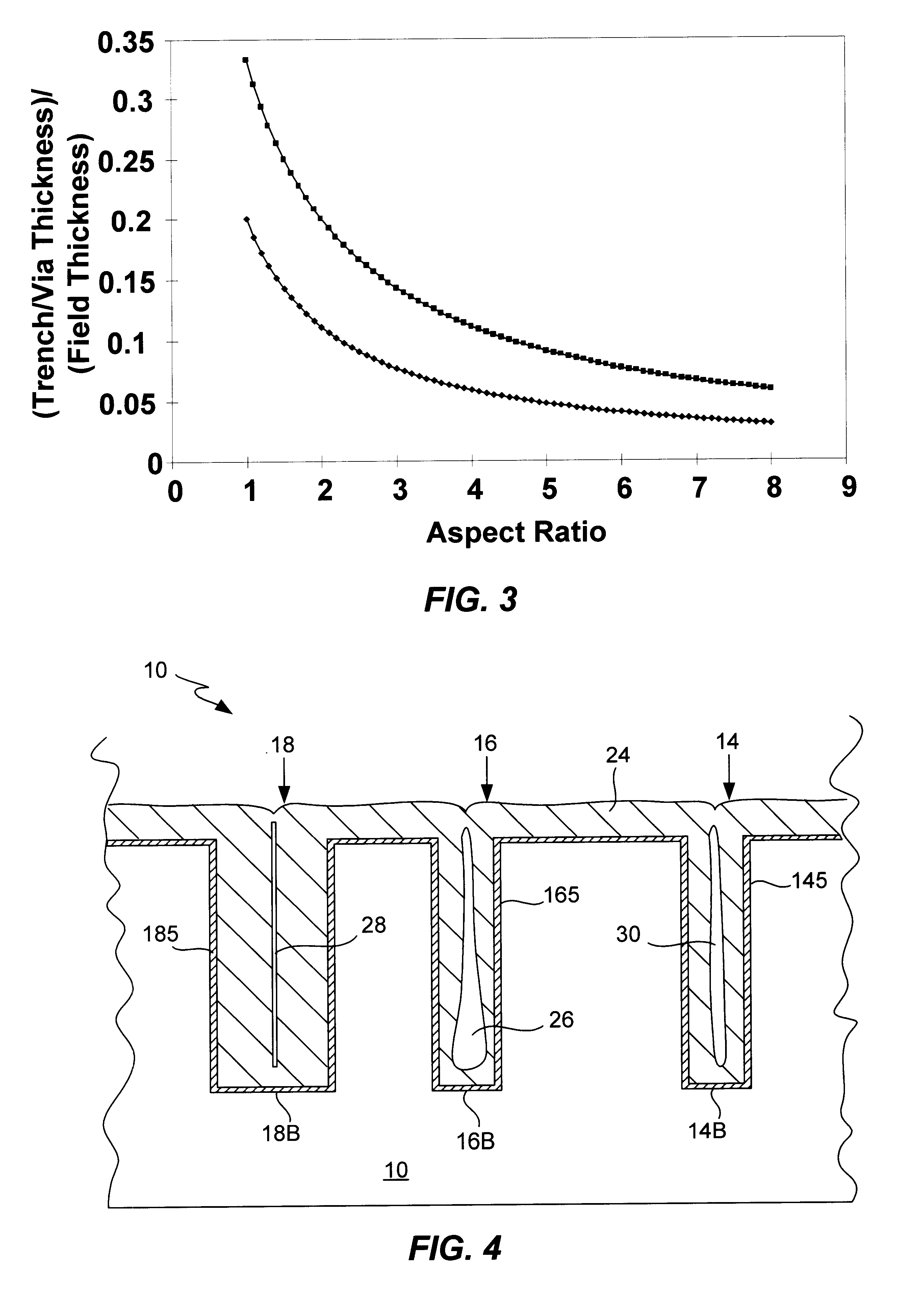
[0074]In the following description and figures, similar reference numbers are used to identify similar elements.

[0075]The present invention is directed towards the plating of copper onto the surfaces of high AR features as would typically be encountered in the fabrication of integrated circuits. However, it is not the intent of the present inventors that the invention be inherently so limited. Procedures described herein will find application in other areas of the field of electrodeposition. However, to provide concrete and definite expression, we describe in detail herein, the plating of copper.

[0076]Typical electroplating baths will contain the metal to be plated, the associated anions in a typically acid solution. Copper electroplating is typically performed from a solution of CuSO4 dissolved in an aqueous solution of sulfuric acid. In addition to these major constituents of the plating bath, it is common for plating baths to contain several additives. “Additives” is intended to ...


PUM

PropertyMeasurementUnit
voltageaaaaaaaaaa
thicknessaaaaaaaaaa
current densityaaaaaaaaaa

Abstract

Several techniques are described for reducing or mitigating the formation of seams and/or voids in electroplating the interior regions of microscopic recessed features. Cathodic polarization is used to mitigate the deleterious effects of introducing a substrate plated with a seed layer into an electroplating solution. Also described are diffusion-controlled electroplating techniques to provide for bottom-up filling of trenches and vias, avoiding thereby sidewalls growing together to create seams/voids. A preliminary plating step is also described that plates a thin film of conductor on the interior surfaces of features leading to adequate electrical conductivity to the feature bottom, facilitating bottom-up filling.

Description

REFERENCE TO RELATED APPLICATION[0001]This application is a divisional of U.S. Application Ser. No. 09 / 410,170 filed on Sep. 30, 1999, now abandoned which claims priority from United States Provisional Patent Application 60 / 105,699, filed Oct. 26, 1998, which is incorporated herein by reference.BACKGROUND OF THE INVENTION[0002]1. Technical Field[0003]This invention relates to electroplating and, in particular, to electrochemical deposition of metals, most particularly to the electrochemical deposition of copper into microscopic recessed features such as high aspect ratio trenches and vias as may occur in the fabrication and packaging of integrated circuits.[0004]2. Description of Related Art[0005]The art of integrated circuits is moving irresistibly towards increased density of components and faster operating speeds. One problem encountered in decreasing the size of components fabricated on an integrated circuit relates to the conductivity of metallic interconnections. Conventional ...

Claims


Application Information

Patent Timeline
Patent Type & Authority Patents(United States)
IPC IPC(8): C25D3/38C25D5/18C25D5/00H05K3/42
CPCC25D3/02C25D3/38C25D5/022C25D5/18H01L21/2885H01L21/76877H05K3/423C25D5/617
Inventor MAYER, STEVEN T.BHASKARAN, VIJAYPATTON, EVAN E.JACKSON, ROBERT L.REID, JONATHAN
Owner NOVELLUS SYSTEMS
Why Eureka
Try Eureka