Self-aligned buried strap process using doped HDP oxide

Inactive Publication Date: 2005-09-20
QIMONDA
View PDF12 Cites 5 Cited by
  • Summary
  • Abstract
  • Description
  • Claims
  • Application Information

AI Technical Summary

Benefits of technology

[0008]To further shrink the vertical DRAM cell, with the invention, the lateral outdiffusion of the buried strap is reduced to avoid interaction between adjacent DRAM cells, while still maintaining a low resistive path to the channel region of the vertical transistor. By reducing the thermal budget of the entire process, the invention outdiffuses dopant from the doped TTO layer and reduces the outdiffusion of the buried strap. Thus, both lateral and vertical outdiffusions are reduced. Sufficient overlap between the buried strap and the transistor channel is not assured with conventional processes that only rely upon outdiffusion from the trench conductor and the node strap to form the buried strap. This is why a portion of the TTO is doped in the inventive structure. In addition, the inventive HDP-CVD TTO deposition process was developed to provide good dopant control in the oxide, to consistently achieve this structure.

Problems solved by technology

In case of planar logic and DRAM devices, short channel effects limit device performance.

Method used


Image

  • Self-aligned buried strap process using doped HDP oxide
  • Self-aligned buried strap process using doped HDP oxide
  • Self-aligned buried strap process using doped HDP oxide

Examples


Embodiment Construction

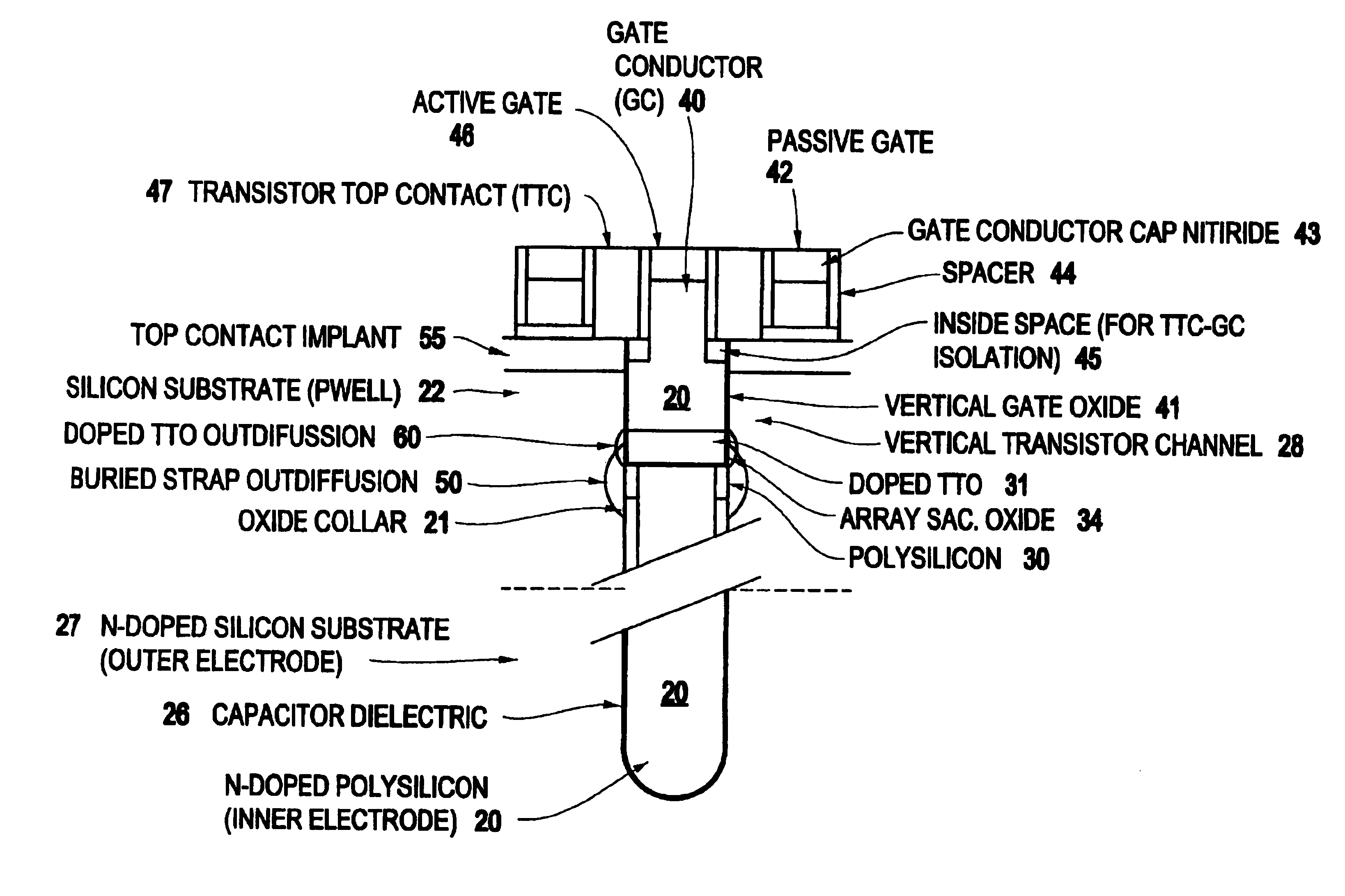
[0020]With further shrinking of groundrules for LOGIC and DRAM devices, development of shallow junctions becomes feasible. The invention uses doped oxides (e.g., As P, etc.) as dopant sources for solid state outdiffusion, thereby allowing processing of shallow junctions.

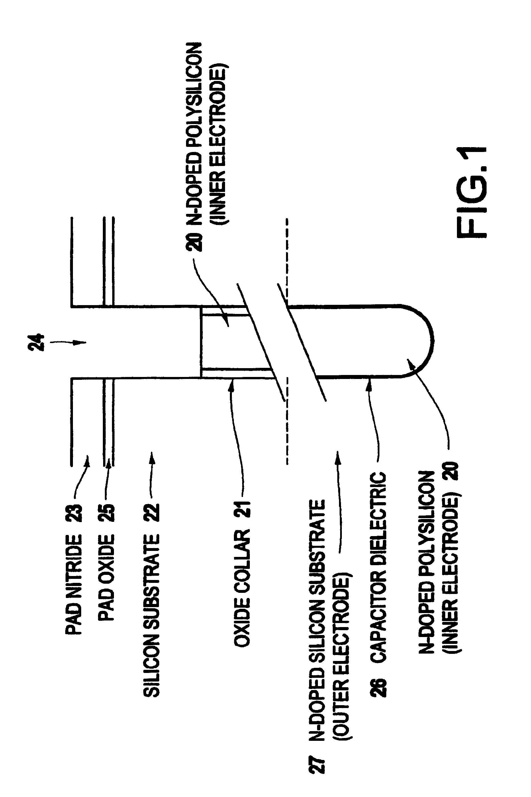
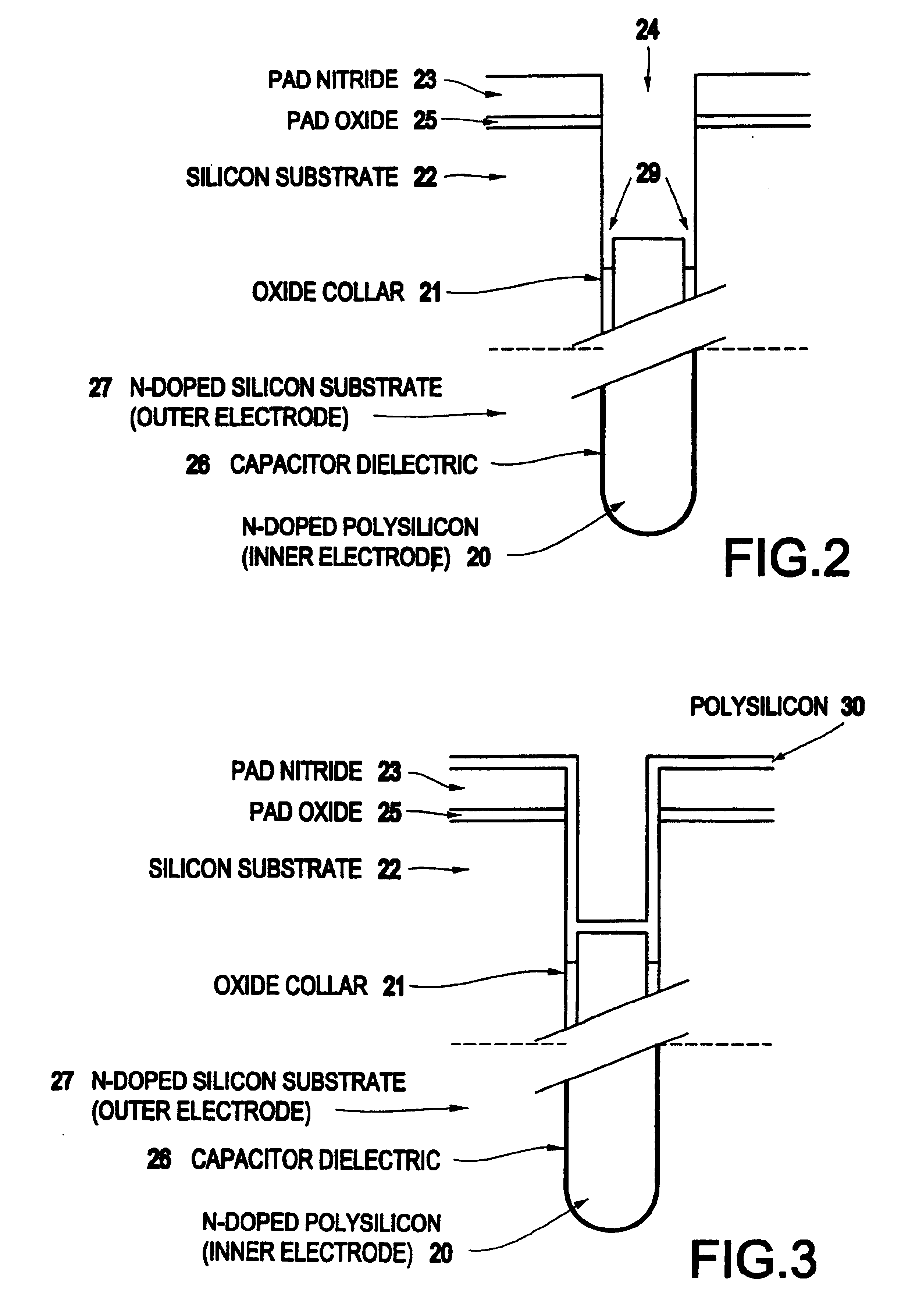
[0021]More specifically, FIG. 1 illustrates the very upper and very lower portions of a deep trench 24 formed in a substrate (e.g., single crystal silicon) structure 22 having a dielectric (e.g., pad nitride 23, formed by chemical vapor deposition (CVD) or physical vapor deposition (PVD) and thermally grown pad oxide 25) upper pad surface. The trench 24 can be formed using any well-known formation and patterning techniques.

[0022]To form the capacitor a dielectric film 26 is deposited or grown in the deep trench 24. Then, the deep trench 24 is filled with a conductive trench node material 20, such as N+doped polysilicon, the upper portion of which is surrounded by a collar dielectric 21 (e.g., oxide). The outer electr...


PUM


Abstract

The invention provides a trench storage structure that includes a substrate having a trench, a capacitor conductor in the lower part of the trench, a conductive node strap in the trench adjacent the capacitor conductor, a trench top oxide above the capacitor conductor, and a conductive buried strap in the substrate adjacent the trench top oxide. The trench top oxide includes a doped trench top oxide layer above the conductive strap, and an undoped trench top oxide layer above the doped trench top oxide layer.

Description

CROSS-REFERENCE TO RELATED APPLICATIONS[0001]This application is a division of U.S. application Ser. No. 10 / 249,228 filed Mar. 24, 2003 now U.S. Pat. No. 6,667,504.BACKGROUND OF INVENTION[0002]The present invention generally relates to the formation of vertical, shallow, and lightly doped, junctions for a vertical transistor, and more particularly to an improved method / structure that makes it possible to process a buried contact with reduced outdiffusion while still maintaining sufficient overlap between the buried contact and the transistor channel.[0003]With further shrinking of groundrules for logic and dynamic random access memory (DRAM) devices, development of improvements becomes necessary. In case of planar logic and DRAM devices, short channel effects limit device performance. For DRAMs with vertical access transistor, the buried contact outdiffusion has to be reduced for isolation reasons, but connectivity to the select transistor must be assured. The invention described be...

Claims


Application Information

Patent Timeline
IPC IPC(8): H01L29/66H01L21/70H01L21/8242H01L29/94
CPCH01L27/10867H01L29/945H01L27/10864H10B12/0383H10B12/0385
Inventor BEINTNER, JOCHENBERGNER, WOLFGANGCONTI, RICHARD A.KNORR, ANDREASWEIS, ROLF
Owner QIMONDA
Why Eureka
Try Eureka