Thermal interface material

a technology of thermal interface material and thermal conductivity, which is applied in the direction of cooling/ventilation/heating modification, semiconductor/solid-state device details, semiconductor devices, etc., can solve the problems of poor soakage effect, polymer matrix loses its original performance, and polymer matrix becomes stiffer and less flexible, etc., to achieve high thermal conductivity

Inactive Publication Date: 2005-09-20
HON HAI PRECISION IND CO LTD
View PDF22 Cites 54 Cited by
  • Summary
  • Abstract
  • Description
  • Claims
  • Application Information

AI Technical Summary

Benefits of technology

[0006]Accordingly, an object of the present invention is to provide a thermal interface material which is thin, and which has a high thermal conductivity.

Problems solved by technology

A typical thermal conductivity of the conventional thermal interface materials is only about 1 W / mK, since the polymer matrix has poor thermal conductivity.
However, adding thermally conductive fillers into the polymer matrix helps only up to a point.
If too many thermally conductive fillers are added, the polymer matrix loses its original performance.
In particular, the polymer matrix can become stiffer and less flexible, and the soakage effect may be worsened.
The thermally conductive characteristics of thermal interface materials have thus been limited for the above reasons.

Method used


Image

  • Thermal interface material
  • Thermal interface material

Examples


Embodiment Construction

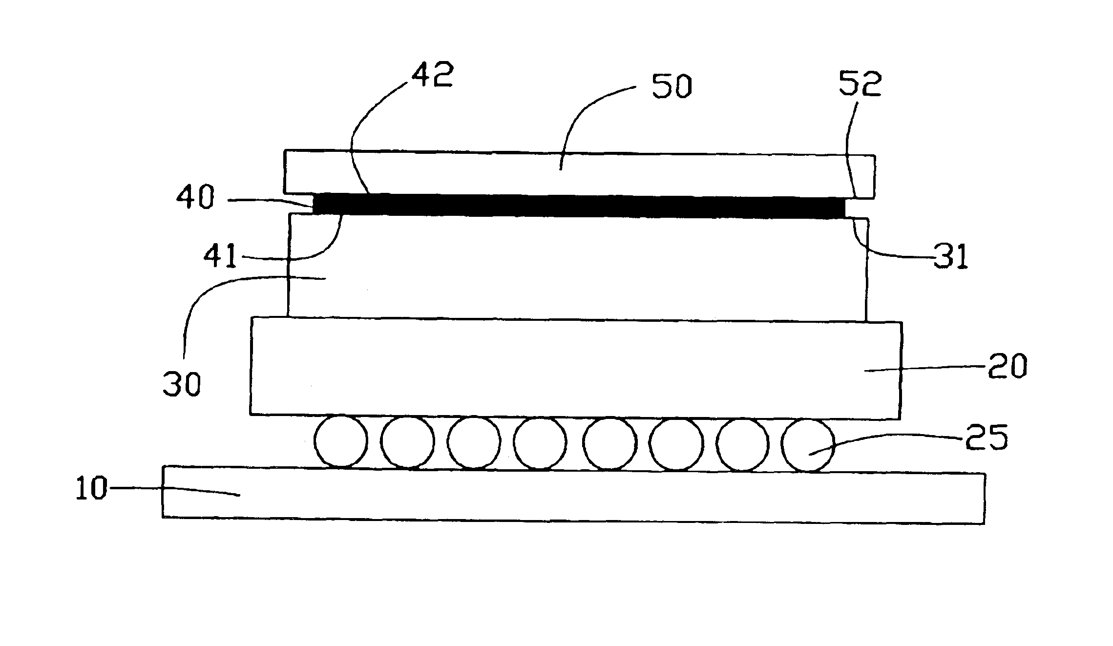
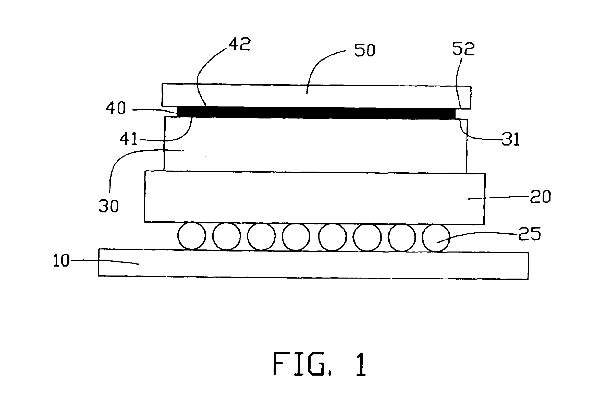
[0010]The following description of illustrative examples and embodiments of the present invention is in connection with an electronic assembly, in which a semiconductor chip (that is a beat source) is positioned on a printed circuit board. However, the present invention is not limited to such kinds of electronic assemblies, nor indeed the electronic assembly shown in FIG. 1. The thermal interface material of the present invention can provide a maximum contact area with a heat source and a heat sink, even if the heat source and / or the heat sink has rough or uneven contact surfaces. The thermal interface material is still efficacious in transferring heat from the heat source to the heat sink.

[0011]The following illustrative examples and embodiments in their various aspects demonstrate that the present invention provides a thermal interface material which can quickly transfer heat away from a high concentration heat source to another suitable location, such as a heat dissipation device...


PUM

PropertyMeasurementUnit
diameteraaaaaaaaaa
diameteraaaaaaaaaa
diameteraaaaaaaaaa

Abstract

A thermal interface material (40) includes a polymer matrix and a number of carbon nanocapsules incorporated in the polymer matrix. The thermal interface material is sandwiched between a heat source (30) having a high density and a heat sink (50). The thermal interface material can provide a maximum surface contact area and can increase thermal conductivity between the heat source and the heat sink.

Description

BACKGROUND OF THE INVENTION[0001]1. Field of the Invention[0002]The present invention relates to a thermal interface material, and especially to a thermal interface material having carbon nano-capsules contained therein. The thermal interface material can be used for transferring heat away from a heat source to a heat sink or other heat dissipation device.[0003]2. Description of Related Art[0004]Recent advances in high speed semiconductor integrated circuit technology have resulted in semiconductor devices which are smaller and run faster than ever before. Such semiconductor devices also generate more heat than ever before. In order to ensure good performance and reliability of the semiconductor devices, their operational temperatures must be kept within a suitable range. Typically, a heat sink is attached to a surface of a semiconductor device, such as a central processing unit (CPU), so that heat is transferred from the semiconductor device to ambient air via the heat sink. When a...

Claims


Application Information

Patent Timeline
Patent Type & Authority Patents(United States)
IPC IPC(8): H01L23/34H01L23/373
CPCH01L23/3737H01L2224/73253H01L2224/16H01L2924/00014H01L2224/0401
Inventor CHEN, GA-LANELEU, CHARLES
Owner HON HAI PRECISION IND CO LTD
Why Eureka
Try Eureka