

Semiconductor memory device
a semiconductor and memory device technology, applied in the direction of information storage, static storage, digital storage, etc., can solve the problems of difficult to effectively reduce the current consumption associated with the refresh operation, difficult to effectively extend the refresh cycle, and limited time for each refresh operation, so as to reduce the self-refresh current
- Summary
- Abstract
- Description
- Claims
- Application Information
AI Technical Summary
Benefits of technology
Problems solved by technology
Method used
Image


Examples
first embodiment
(First Embodiment)
[0061]The first embodiment of the present invention will be described. A semiconductor memory device according to the first embodiment is a pseudo SRAM which uses the same memory cells as the DRAM (dynamic random access memory), and which is operable in accordance with the same specification as the SRAM (static random access memory), wherein the pseudo SRAM is configured so that a detection is made of an address or a chip select signal externally inputted, thereby to generate an internal pulse signal, whereby the refresh operation and the read and write operations are sequentially conducted in the same cycle by triggering this pulse signal. In this invention, “read / write operation” means any of “read operation” and “write operation”.
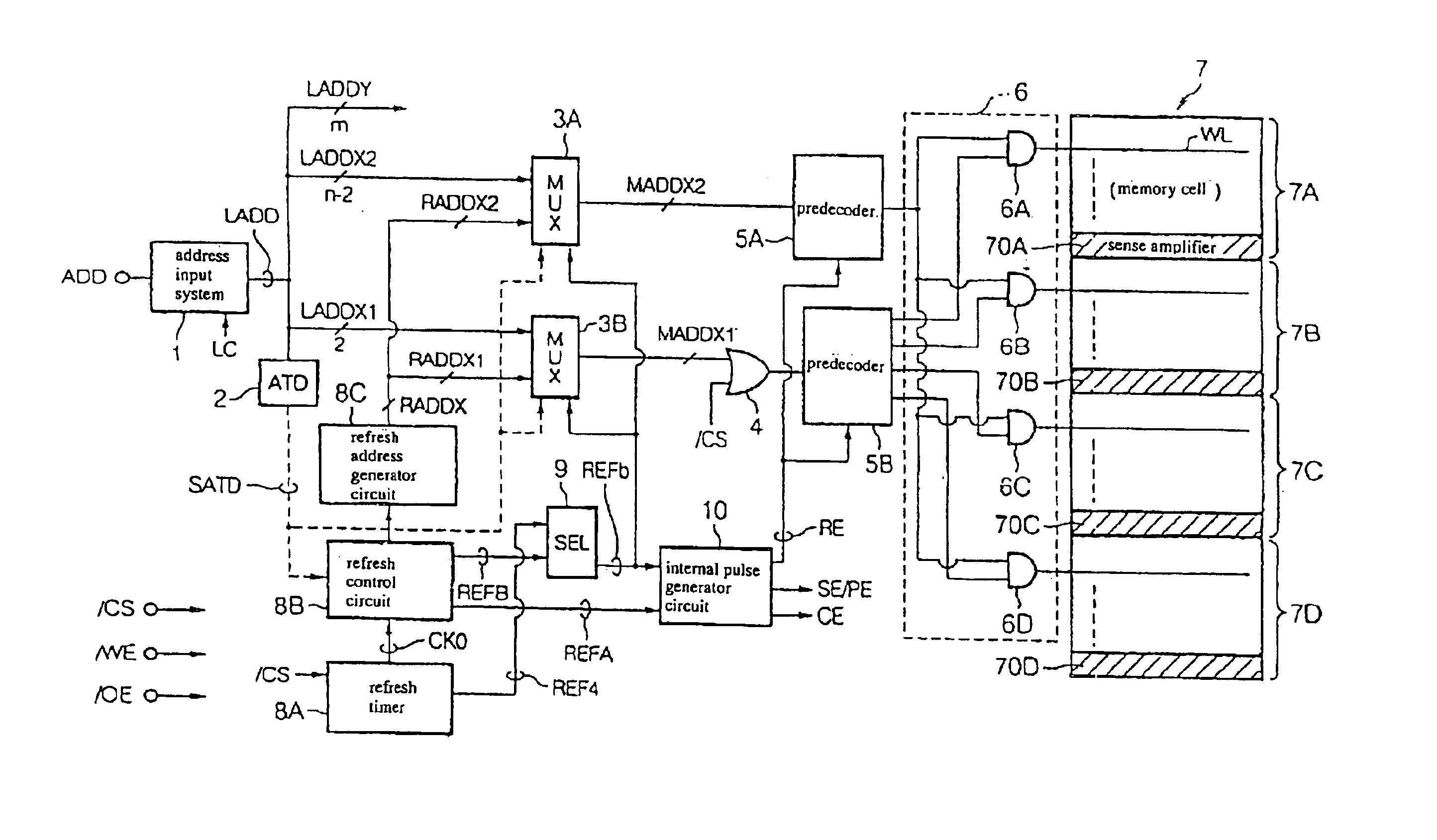
[0062]FIG. 1 shows an entire configuration of the semiconductor memory device in accordance with this embodiment.
[0063]In this drawing, an address ADD is a signal given from the outside to this semiconductor memory device, and includes ...
second embodiment
(Second Embodiment)
[0128]The second embodiment of the present invention will be described.
[0129]In the above-described first embodiment, switch of the operation mode from the active mode to the stand-by mode is detected to additionally execute the refresh in the stand-by mode. In accordance with this second embodiment, even if the operation mode is switched to the stand-by mode, after the refresh operation is completed to the group of the word lines, which should be refreshed in the active mode, then the four word lines are selected in parallel for refresh operation.
[0130]FIG. 8 shows the configuration of the semiconductor memory device of this second embodiment. This semiconductor memory device is different in configuration from the configuration shown in FIG. 1 in the first embodiment in view that a logic gate 90 is provided instead of the selector 90, and a refresh timer 8D is provided instead of the refresh timer 8A, and a refresh control circuit 8E is provided instead of the re...
third embodiment
(Third Embodiment)
[0141]In this third embodiment, operations of driving the word lines will be described when the operation mode is switched during the refresh operation, and the refresh operation is thus interrupted. In the refresh operation, the word line is selected so that data in the memory cells are read out and transferred onto the bit lines for subsequent amplification by the sense amplifiers and the amplified data are then re-stored in the memory cells. It takes a time from selecting the word line until a potential difference, which can be amplified by the sense amplifier, appears on the bit line. Activation of the sense amplifier is made after a predetermined time has passed from selecting the word line.
[0142]Accordingly, it is temporary caused that an internal node of the memory cell is electrically connected to the bit line without activation of the sense amplifier. In this state, a charge accumulated as a datum in the memory cell is consumed to charge and discharge the ...
PUM
 Abstract
Description
Claims
Application Information