Duel-layer optical scanner with non-periodic phase structure element of birefringent material for different wavefront aberration compensation of orthogonally polarized radiation beams

a birefringent material and scanning device technology, applied in the direction of optical beam sources, instruments, lenses, etc., can solve the problems of increasing the cost of scanning device manufacture, deteriorating the resolution of optical spots formed, and relatively complex production of periodic phase structures, i.e. gratings, etc., and achieve the effect of reducing astigmatism

Inactive Publication Date: 2005-09-20
KONINKLIJKE PHILIPS ELECTRONICS NV
View PDF10 Cites 17 Cited by
  • Summary
  • Abstract
  • Description
  • Claims
  • Application Information

AI Technical Summary

Benefits of technology

[0011]It is noted that a similar effect could be achieved using birefringent lenses instead of a step-like structure; however the arrangement of the present invention has an advantage in that astigmatism can be reduced; birefringent lenses in general give rise to astigmatism wavefront aberration, because rays do not travel parallel to the optical axis of the lens.
[0012]It should be noted that the phase structure according to the invention has a non-periodic pattern, i.e. one which does not regularly repeat in the radial direction, and, therefore, does not form diffraction orders. As a consequence, the phase structure does not have the inherent losses of a grating. The optical element introduces the required wavefront changes without appreciable loss of radiation energy.

Problems solved by technology

Without compensating measures, refocusing from one layer to the other results in spherical aberration, generating a wavefront error of 200-300 mλ (rms), which deteriorates the resolution of the optical spot formed.
However, using mechanical actuators to provide spherical aberration compensation, particularly when a separate mechanical actuator is used to provide focus control, is relatively complex and therefore increases the cost of manufacture of the scanning device.
One drawback is that the production of the periodic phase structure, i.e. the grating, is relatively complex due to the large number of elements within the structure.
Furthermore, due to the diffraction, a certain amount of the input light is wasted, which is undesirable.

Method used


Image

  • Duel-layer optical scanner with non-periodic phase structure element of birefringent material for different wavefront aberration compensation of orthogonally polarized radiation beams
  • Duel-layer optical scanner with non-periodic phase structure element of birefringent material for different wavefront aberration compensation of orthogonally polarized radiation beams
  • Duel-layer optical scanner with non-periodic phase structure element of birefringent material for different wavefront aberration compensation of orthogonally polarized radiation beams

Examples


Embodiment Construction

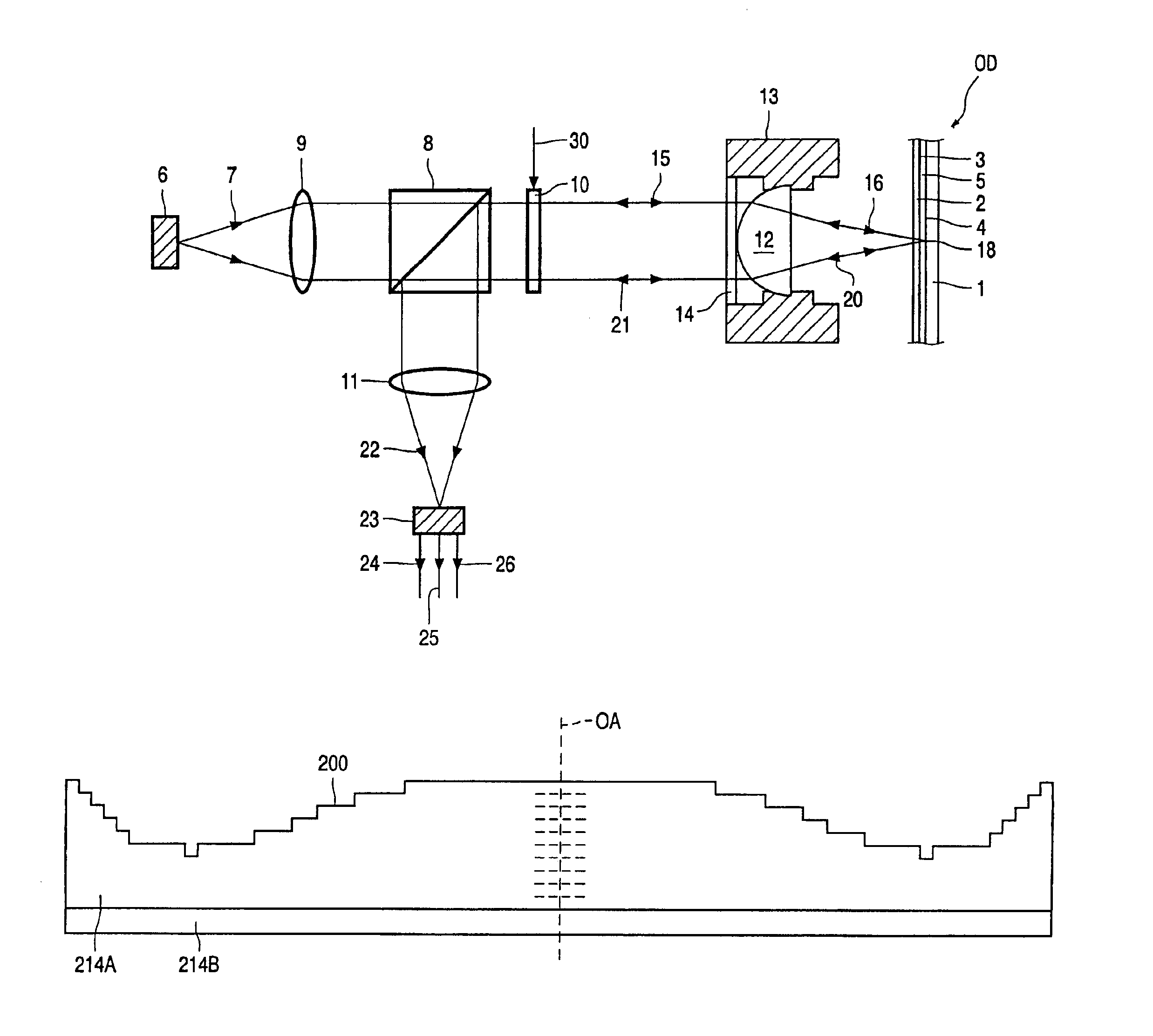
[0021]FIG. 1 is a schematic illustration of components common to a device, in accordance with each of the embodiments of the invention described by way of example below, for scanning an optical record carrier. The record carrier is for example an optical disk as will be described, by way of example, below.

[0022]The optical disk OD comprises a substrate 1 and a transparent layer 2, between which at least one information layer 3 is arranged. In the case of a dual-layer optical disk, as illustrated, two information layers 3, 4 are arranged behind the transparent layer 2, at different depths within the disk, separated by 20 μm (±10 μm). A further transparent layer 5 separates the two information layers. The transparent layer 2, having a thickness of approximate 80 μm (±30 μm), has the function of protecting the uppermost information layer 3, while the mechanical support is provided by the substrate 1.

[0023]Information may be stored in the information layers 3, 4 of the optical disk in t...


PUM

PropertyMeasurementUnit
thicknessaaaaaaaaaa
thicknessaaaaaaaaaa
thicknessaaaaaaaaaa

Abstract

An optical scanning device for scanning a dual-layer optical record carrier with dual orthogonally polarized radiation beams. The device having a spherical aberration compensation optical subsystem including a switchable liquid crystal cell of birefringent material for altering different optical paths lengths provided by a phase structure of stepped annular zones.

Description

FIELD OF THE INVENTION[0001]This invention relates to an optical scanning device, and an optical element for use therein, for scanning an optical record carrier, such as an optical disk, comprising an information layer, the device comprising a radiation source for generating a radiation beam and an objective lens, located in an optical path between the radiation source and the information layer, for converging the radiation beam to a spot on the information layer. In particular, but not exclusively, the invention relates to an optical scanning device including an optical element to compensate for spherical aberrations generated by different optical path lengths (referred to herein as information layer depths) through which the beam travels in an optical disk to reach an information layer in the disk.BACKGROUND OF THE INVENTION[0002]There is a need for the production of optical record carriers of high capacity. Therefore, optical scanning devices using a relatively short wavelength r...

Claims


Application Information

Patent Timeline
Patent Type & Authority Patents(United States)
IPC IPC(8): G11B7/125G11B7/135G11B7/00
CPCG11B7/1367G11B7/13925G11B2007/0013
Inventor HENDRIKS, BERNARDUS HENDRIKUS WILHELMUSDE VRIES, JORRIT ERNSTSTALLINGA, SJOERD
Owner KONINKLIJKE PHILIPS ELECTRONICS NV
Why Eureka
Try Eureka