Semiconductor memory device

a memory device and semiconductor technology, applied in the field of semiconductor memory devices, can solve the problems of data in the memory area remaining destroyed, and achieve the effect of suppressing the power consumption of the memory device and boosting the voltage of the word lin

Inactive Publication Date: 2005-09-27
FUJITSU SEMICON LTD
View PDF1 Cites 42 Cited by
  • Summary
  • Abstract
  • Description
  • Claims
  • Application Information

AI Technical Summary

Benefits of technology

[0019]According to one aspect of the present invention, there is provided an FeRAM wherein after a read operation is conducted to a memory area designated by an address, a bit line is pre-charged with a ground potential and then an electric potential of a plate line is lowered, thereby stopping the data from being written back to an area the data of which is destroyed by the read operation. In the FeRAM, the electric potential of the word line may be kept at VDD Level without boosting it to a potential for writing back the data. Alternatively, the bit line is clamped to the g

Problems solved by technology

Therefore, the data in the m

Method used


Image

  • Semiconductor memory device
  • Semiconductor memory device
  • Semiconductor memory device

Examples


Embodiment Construction

[0053]Exemplary embodiments of the present invention are explained hereinafter in detail with reference to the accompanying drawings.

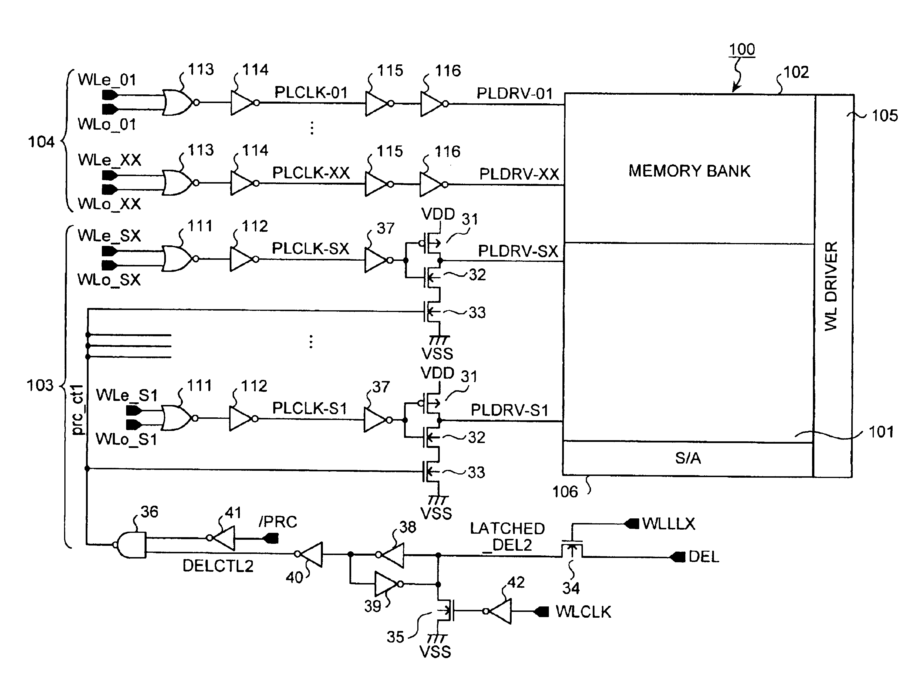
[0054]FIG. 9 is a schematic diagram that shows the overall configuration of a semiconductor memory device according to the present invention. This memory device (that is, a semiconductor memory device) 20 includes a nonvolatile memory block 21 that consists of a ferroelectric memory, a memory block peripheral circuit 22 that consists of, for example, an X decoder circuit, a Y decoder circuit, a sense amplifier and the like to control a data write operation, a data read operation, a data deletion operation or the like for the memory block 21, and an I / O Interface 23 for the input / output of data to and from the memory block 21. In addition, the semiconductor memory device 20 includes various control signal lines, respectively, and a data bus 27. An address signal is input into a control signal line 24, a data destructive signal DEL is input into a contro...


PUM


Abstract

After a read operation is conducted to a memory area designated by an address in response to a combination of a data destructive signal and a chip select signal, a bit line is pre-charged with a ground potential and an electric potential of a plate line is lowered, thereby stopping the data from being written back to an area in which the data is destroyed by the read operation. The electric potential of the word line may be kept at VDD level without boosting it to a potential for writing back the data. The bit line may be clamped to the ground potential, thereby stopping the read data from being output to an outside of a memory device to stop an operation of a sense amplifier.

Description

CROSS-REFERENCE TO RELATED APPLICATIONS[0001]This application is based upon and claims the benefit of priority from the prior Japanese Patent Application No.2002-241109, filed on Aug. 21, 2002, the entire contents of which are incorporated herein by reference.BACKGROUND OF THE INVENTION[0002]1) Field of the Invention[0003]The present invention relates to a semiconductor memory device that consists of a ferroelectric memory.[0004]2) Description of the Related Art[0005]A ferroelectric memory is a nonvolatile memory that uses a ferroelectric material for a capacitor film and that stores data by the residual polarization of the ferroelectric material. Since it is unnecessary to use a power supply to hold data, the ferroelectric memory may be applied to a storage device that stores and holds data in an IC card. In the future, multi-purpose IC card obtained by incorporating various applications into a single IC card may be considered. In a multi-purpose IC card of this type, a storage dev...

Claims


Application Information

Patent Timeline
IPC IPC(8): G11C11/22
CPCG11C11/22
Inventor SUZUKI, HIDEAKI
Owner FUJITSU SEMICON LTD
Why Eureka
Try Eureka