Method of manufacturing a surface acoustic wave element

a surface acoustic wave and manufacturing method technology, applied in the direction of device material selection, device details, instruments, etc., can solve the problems of electrode pattern damage, deterioration in characteristics, discharge, etc., to prevent the electrode pattern from being damaged.

Inactive Publication Date: 2005-10-04
PANASONIC CORP
View PDF8 Cites 11 Cited by
  • Summary
  • Abstract
  • Description
  • Claims
  • Application Information

AI Technical Summary

Benefits of technology

[0012]As described above, according to the present invention, all the electrode patterns are directly and indirectly connected by using connecting electrodes and short-circuit electrodes, thereby not allowing any electrodes to be electrically freed. In this way, the potential for electric charge to be generated on the piezoelectric substrate is made uniform over the entire piezoelectric substrate, making it free from potential difference, and it is also possible to prevent the electrodes from being damaged by static discharge and the like.

Problems solved by technology

When the accumulated charge exceeds a certain level, discharge takes place between the electrodes, such as the IDT electrodes, causing the electrode pattern to be damaged and deteriorated in characteristics.
Therefore, it becomes difficult to design so as to achieve the intended filter function for a SAW device.
Further, since the IDT electrode finger is not wide enough and the impedance is great, the potential cannot be made sufficiently uniform, sometimes causing discharge to take place when a big electric charge is generated.

Method used


Image

  • Method of manufacturing a surface acoustic wave element
  • Method of manufacturing a surface acoustic wave element
  • Method of manufacturing a surface acoustic wave element

Examples


first exemplary embodiment

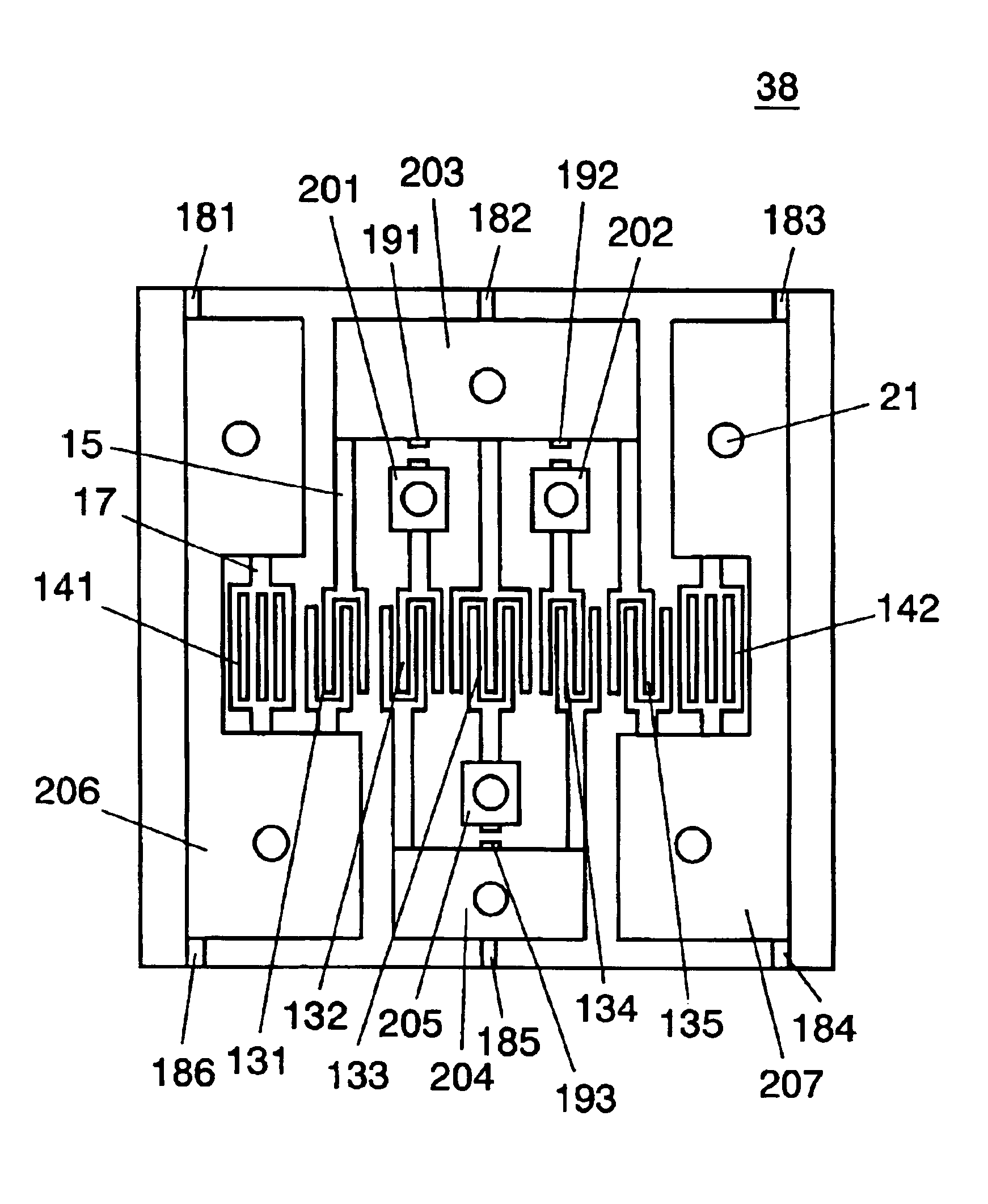
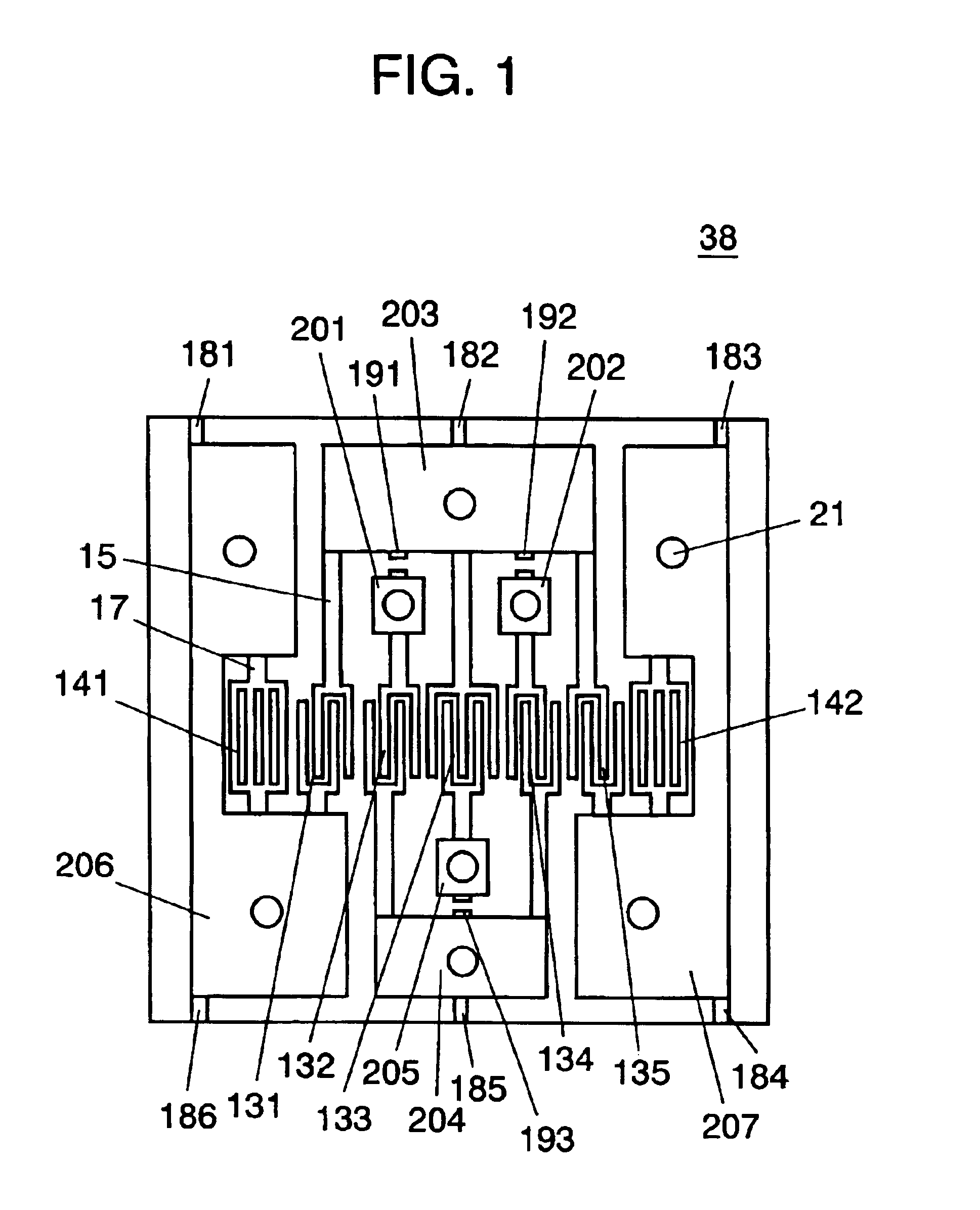
[0037]FIG. 1 is a plan view showing an individual piece of a diced piezoelectric substrate having an electrode pattern configuration of a SAW element in a first exemplary embodiment of the present invention.

[0038]A metal film, such as a single layer of Al, Al-alloy or titanium (Ti), or a laminated layer of these, is formed on piezoelectric substrate 11 made up of LiTaO3 single crystal substrate or the like. A SAW element including a predetermined IDT electrode, grating reflector electrodes on either side of the IDT electrode, and pad electrodes led from the grating reflector electrodes is formed through a photolithography process and an etching process.

[0039]In the first exemplary embodiment, IDT electrodes including outer IDT electrodes 131, 135, inner IDT electrodes 132, 134, and central IDT electrode 133 are formed. Also, terminal electrodes 15 lead from each of these electrodes.

[0040]The outer IDT electrodes 131, 135 are each connected at respective first sides thereof to pad el...

second exemplary embodiment

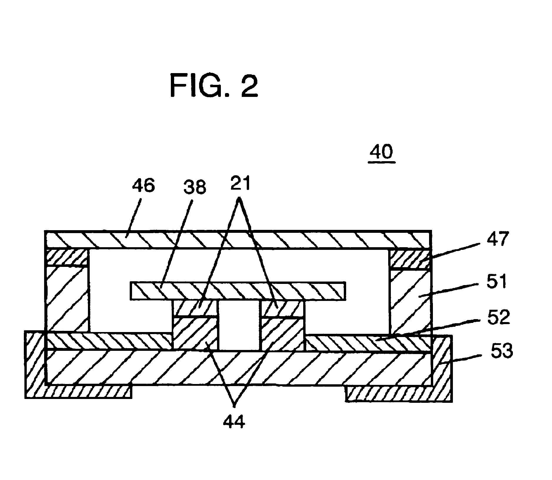
[0074]A second exemplary embodiment of the present invention will be described in the following with reference to the drawings.

[0075]FIG. 5A to FIG. 5E are sectional views showing the manufacturing process of a SAW element in the second exemplary embodiment of the present invention. The same elements as shown in FIG. 1 to FIG. 4E are given the same reference numerals.

[0076]The difference between the first exemplary embodiment and the second exemplary embodiment with respect to the manufacturing method is that in the second embodiment, the pad reinforcing electrodes 201, 202, 203, 204, 205, 206, 207 are formed, and then, after forming the bump 21, all of the connecting electrodes 191, 192, 193 and all of the short-circuit electrodes 181, 182, 183, 184, 185, 186 are removed. Otherwise, the manufacturing process of the second embodiment is the same as in the first exemplary embodiment.

[0077]In other words, in the second exemplary embodiment, FIG. 5A to FIG. 5B is the same as FIG. 3A to...


PUM

PropertyMeasurementUnit
thicknessaaaaaaaaaa
widthaaaaaaaaaa
solubleaaaaaaaaaa

Abstract

A SAW element of the present invention includes a plurality of inter-digital transducer (IDT) electrodes on a piezoelectric substrate, grating reflector electrodes disposed on the sides of the IDT electrodes, and a plurality of pad electrodes led from the IDT electrodes and the grating reflector electrodes. A plurality of the pad electrodes includes isolated pad electrodes not directly opposed to the outer periphery of the SAW element, and adjacent pad electrodes directly opposed to the outer periphery thereof A connecting electrode between the isolated pad electrode and the adjacent pad electrode is removed by etching at least before dicing in order to prevent discharge from occurring due to pyroelectricity, and to prevent the electrodes from being damaged.

Description

FIELD OF THE INVENTION[0001]The present invention relates to a surface acoustic wave device (hereinafter called a SAW device) and a surface acoustic wave element (hereinafter called a SAW element) used in the SAW device for communication equipment, and manufacturing methods thereofBACKGROUND OF THE INVENTION[0002]A conventional SAW device is generally manufactured by the following method. As a piezoelectric substrate, for example, a lithium tantalate (LiTaO3) single crystal substrate is used. A metal film of aluminum (Al) or the like is formed on the piezoelectric substrate, and an inter digital transducer electrode (hereafter called IDT electrode) and a grating reflector electrode are formed by photolithography and an etching process. In this way, after forming several SAW elements on the piezoelectric substrate, the substrate is diced into individual pieces. A SAW device is manufactured by mounting individual SAW elements on a ceramic package or the like. Here, the connection of t...

Claims


Application Information

Patent Timeline
Patent Type & Authority Patents(United States)
IPC IPC(8): H03H9/145H03H9/00H03H3/08H03H9/25H03H9/02H03H3/00
CPCH03H3/08H03H9/02921H03H9/02992Y10T29/49005Y10T29/49156Y10T29/49798Y10T29/49144Y10T29/42Y10T29/49007Y10T29/49128Y10T29/49794
Inventor TOMIOKA, MUNEKOYAMASHITA, KIYOHARUFURUKAWA, MITSUHIRO
Owner PANASONIC CORP
Why Eureka
Try Eureka