Image pickup apparatus
- Summary
- Abstract
- Description
- Claims
- Application Information
AI Technical Summary
Benefits of technology
Problems solved by technology
Method used
Image
Examples
first embodiment
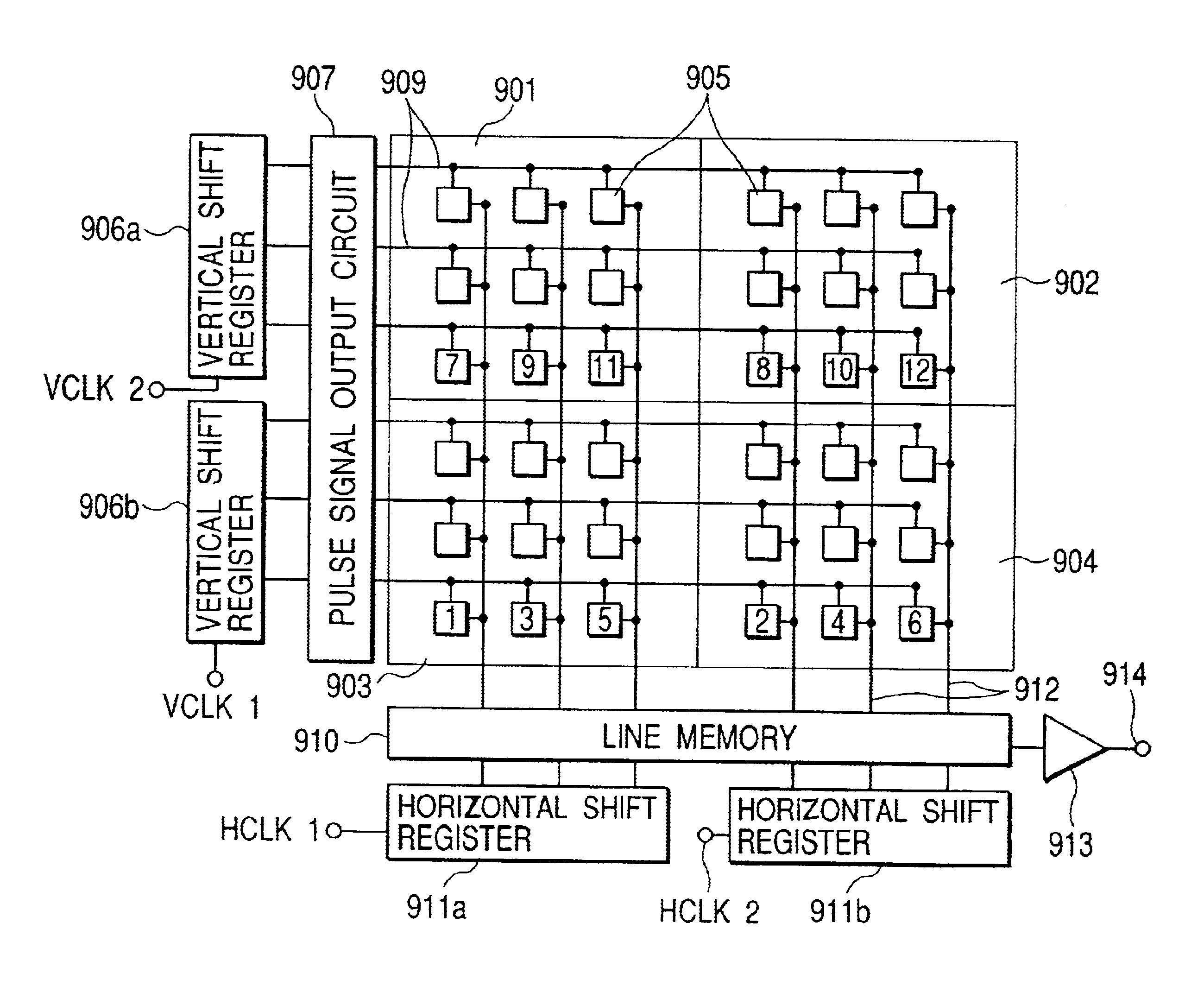
[0054]FIG. 4 is a schematic view showing a configuration of a solid-state image pickup element of the present invention, components of which are formed on a same semiconductor chip by, for example, a CMOS process. In FIG. 4, reference numeral 905 denotes pixels having a photo diode, 901 to 904 denote image pickup areas in which the pixels 905 are arranged two-dimensionally and R, G1, G2 and B filters for forming an image, respectively, are provided, 906a denotes a vertical shift register for outputting a control signal which is generated for controlling pixel scanning in the vertical direction in the image pickup areas 901 and 902, in accordance with a clock signal VCLK2 that is inputted from the outside, 906b denotes a vertical shift register that is signal supplying means for outputting a control signal which is generated for controlling pixel scanning in the vertical direction in the image pickup areas 903 and 904, in accordance with a clock signal VCLK1 that is inputted from the...
second embodiment
[0075]FIG. 6 is a schematic view showing a configuration of a solid-state image pickup element of the present invention, components of which are formed in a same semiconductor chip by the CMOS process or the like. In FIG. 6, reference symbols 910a and 911b denote line memories for accumulating charges or the like read out from the pixels 905 arranged in the R image pickup area 901 and the G1 image pickup area 902, respectively, and 911c to 911f denote horizontal shift registers for sequentially outputting charges or the like read out from the R image pickup area 901, the G1 image pickup area 902, the G2 image pickup area 903 and the B image pickup area 904 among the charges or the like retained in the line memories 910a and 911b to an external processing circuit. Further, in FIG. 6, parts similar to those shown in FIG. 4 are given identical reference numerals.
[0076]In addition, operations of the solid-state image pickup element shown in FIG. 6 are similar to those shown in FIG. 4. H...
third embodiment
[0083]FIG. 7 is a schematic view showing a configuration of a solid-state image pickup element of the present invention. In FIG. 7, reference numeral 905 denotes pixels having photoelectric conversion element, and 901 to 904 denote image pickup areas of R, G1 , G2 and B in which the pixels 905 are arranged two-dimensionally to form an image, respectively, the four image pickup areas being configured to be arranged two-dimensionally. Reference symbols 906a to 906d denote vertical shift registers for controlling timing for supplying a control signal for reading out an amplified signal that is based on a charge from each pixel 905 arranged in each of the image pickup areas 901 to 904, respectively, 909 denotes horizontal signal lines for supplying a control signal to each pixel 905, 912 denotes vertical signal lines for transmitting an amplified signal read out from each pixel 905, and 911a to 911d denote horizontal shift registers for sequentially controlling the transfer of amplified...
PUM
 Abstract
Description
Claims
Application Information


