
Computer CPU and memory to accelerated graphics port bridge having a plurality of physical buses with a single logical bus number

a technology of agp bus and agp port bridge, which is applied in the direction of memory address/allocation/relocation, instruments, computing, etc., can solve the problems of software operating system not being able to configure, the original configuration information stored in the nvram will not be correct for those pci cards now, and the complexity of 3-d graphics requires higher speed access to ever larger amounts of graphics data stored in memory. , to achieve the effect of avoiding multiple delays,

Inactive Publication Date: 2005-10-11
HEWLETT PACKARD DEV CO LP
View PDF16 Cites 2 Cited by
  • Summary
  • Abstract
  • Description
  • Claims
  • Application Information

AI Technical Summary

Benefits of technology

This solution simplifies AGP device identification and configuration, reduces latency, avoids deadlocks, and allows for concurrent transactions, enabling efficient use of multiple high-bandwidth AGP devices without the need for additional AGP bridges, thus enhancing system performance and stability.

Problems solved by technology

Increasingly complex 3-D graphics require higher speed access to ever larger amounts of graphics data stored in memory.
However, situations often arise which require rerunning the system configuration utility to update the device configuration information stored in the NVRAM when a new device is added to the computer system.
This creates a problem since any user configured information such as interrupt request (IRQ) number, etc., stored in the NVRAM specifies the bus and device / function number of the PCI device to which it applies.
If the PCI bus numbers of any of the PCI cards change because a new PCI bus was introduced by adding a new PCI—PCI bridge to the computer, the original configuration information stored in the NVRAM will not be correct for those PCI cards now having different bus numbers, even though they remain in the same physical slot numbers.
This situation results in the software operating system not being able to configure the PCI cards now having bus numbers different than what was expected from the information stored in the NVRAM.
This can be especially bothersome for a PCI device such as a controller which has been configured as a system startup device, but now cannot be used to startup the computer system because its registers have not been initialized during POST to indicate that it is supposed to be the primary controller.
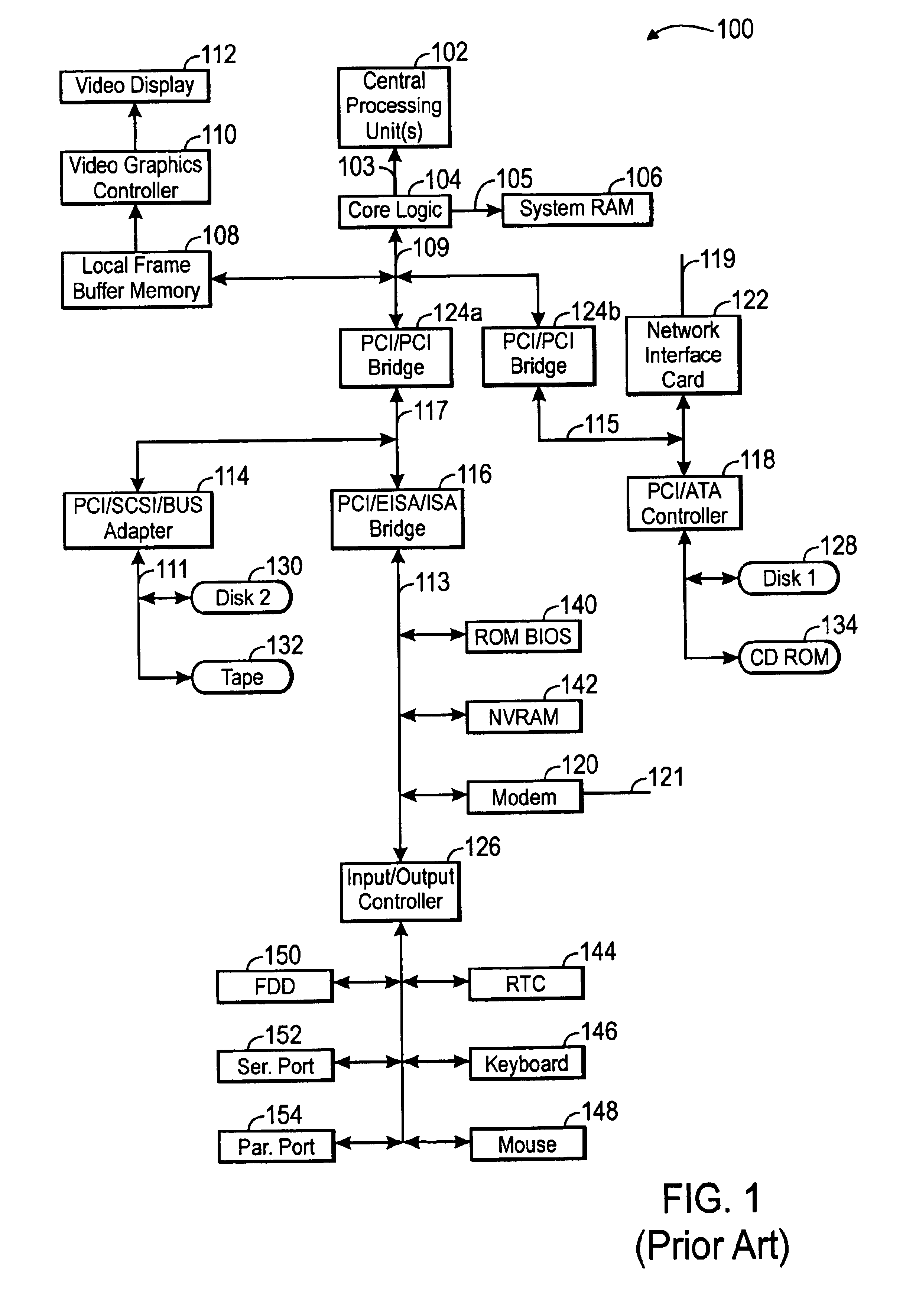
Thus, adding PCI to PCI bridges is not very efficient when 66 MHz operation of the PCI buses is desired.
Sequentially connecting the PCI to PCI bridges causes increased propagation time and bus to bus handshake and arbitration problems.
The number of PCI cards that may he connected to a PCI bus is limited, however, because the PCI bus is configured for high speed data transfers.
If the PCI bus numbers stored in the NVRAM do not match the actual PCI bus numbers, proper computer system operation may be impaired.
A problem may exist, however, in computer systems having one or more high speed central processing units that perform a plurality of host to PCI transactions.
These host to PCI transactions may occur so frequently and quickly that PCI to PCI transactions may be starved due to lack of PCI bus availability.

Method used


Image

  • Computer CPU and memory to accelerated graphics port bridge having a plurality of physical buses with a single logical bus number
  • Computer CPU and memory to accelerated graphics port bridge having a plurality of physical buses with a single logical bus number
  • Computer CPU and memory to accelerated graphics port bridge having a plurality of physical buses with a single logical bus number

Examples


Embodiment Construction

[0079]The following patents are hereby incorporated by reference:

[0080]U.S. Pat. No. 6,175,889, filed Oct. 21, 1998, entitled “Apparatus, Method and System for a Computer CPU and Memory to High Speed Peripheral Interconnect Bridge Having a Plurality of Physical Buses with a Single Logical Bus Number” by Sompong P. Olarig;

[0081]U.S. Pat. No. 5,878,237, filed Jul. 11, 1997, entitled “Apparatus, Method and System for a Computer CPU and Memory to PCI Bridge Having a Plurality of Physical PCI Buses” by Sompong P. Olarig.

[0082]One or more specific embodiments of the present invention will be described below. In an effort to provide a concise description of these embodiments, not all features of an actual implementation are described in the specification. It should be appreciated that in the development of any such actual implementation, as in any engineering or design project, numerous implementation-specific decisions must be made to achieve the developers' specific goals, such as compli...


PUM


Abstract

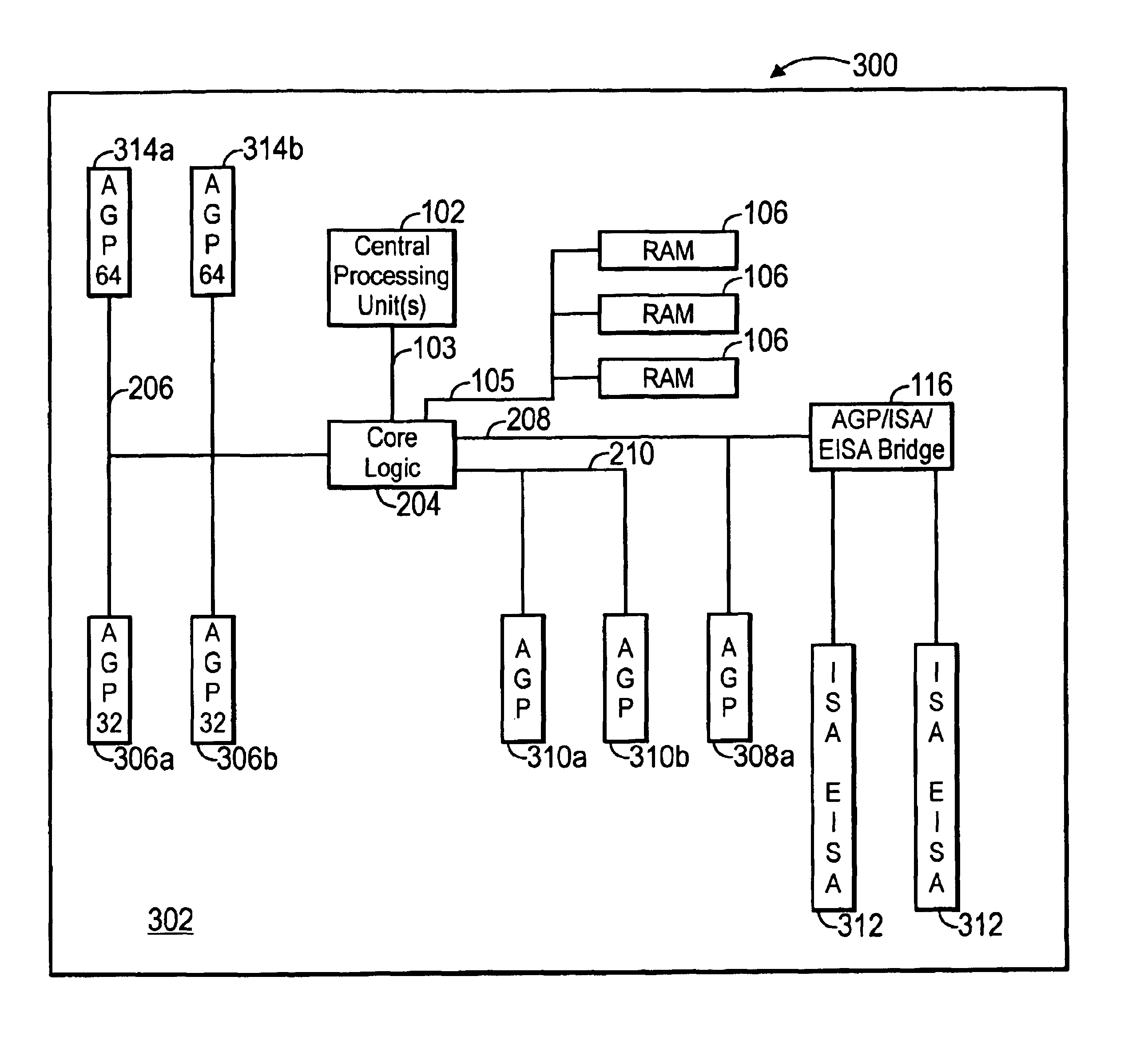
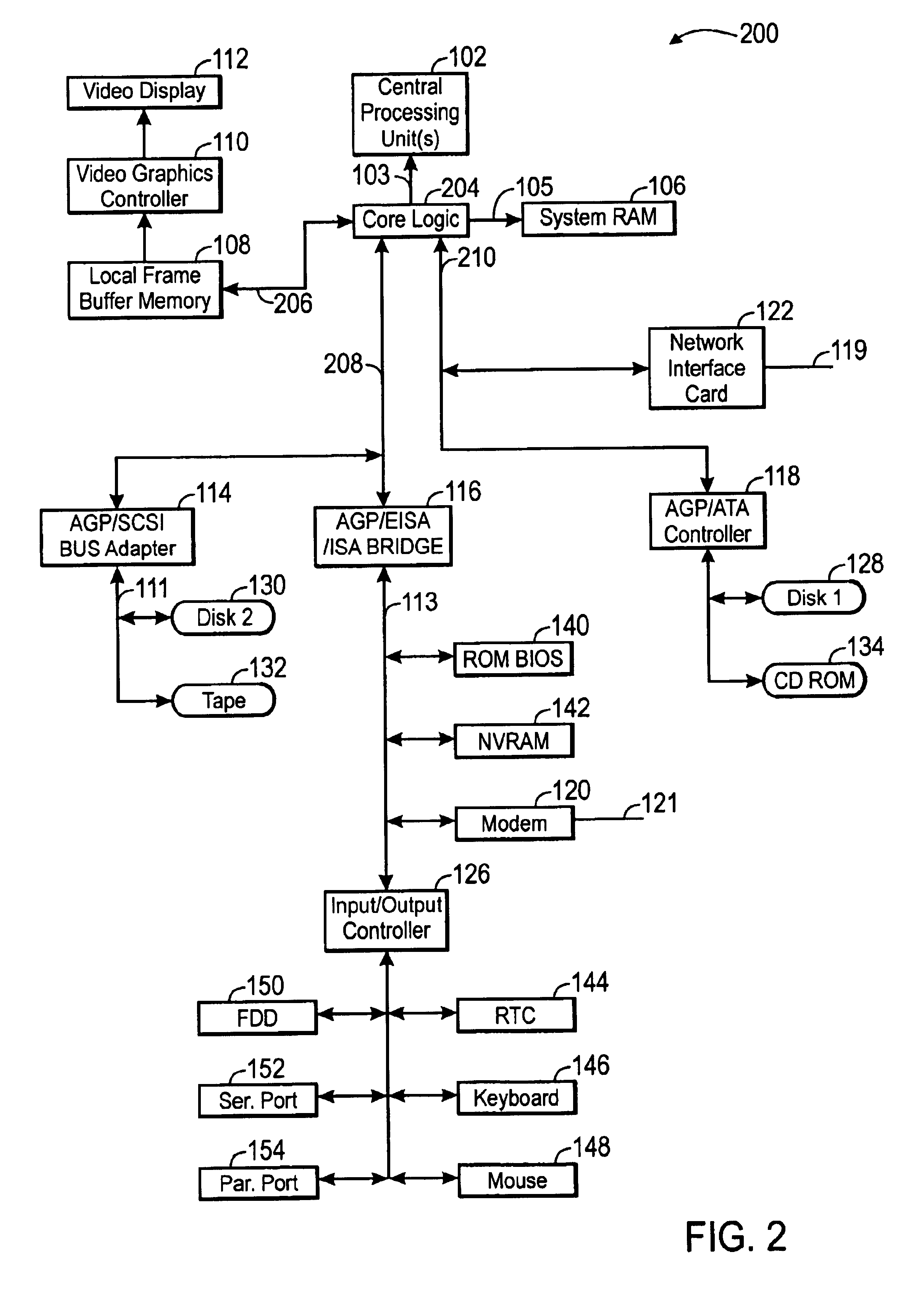
A core logic chip set in a computer system provides a bridge between processor host and memory buses and a plurality of Accelerated Graphics Port (AGP) buses. Each of the plurality of AGP buses have the same logical bus number. The core logic chip set has an arbiter having Request (“REQ”) and Grant (“GNT”) signal lines for each AGP device connected to the plurality of AGP physical buses. Each of the plurality of AGP buses has its own read and write queues to provide transaction concurrency of AGP devices on different ones of the plurality of AGP buses when the transaction addresses are not the same or are M byte aligned. Upper and lower memory address range registers store upper and lower memory addresses associated with each AGP device. Whenever a transaction occurs, the transaction address is compared with the stored range of memory addresses. If a match between addresses is found then strong ordering is used. If no match is found then weak ordering may be used to improve transaction latency times. AGP device to AGP device transactions may occur without being starved by CPU host bus to AGP bus transactions.

Description

CROSS REFERENCE TO RELATED PATENT APPLICATION[0001]This patent application is a continuation-in-part of U.S. patent application Ser. No. 09 / 730,948, filed Dec. 6, 2000, entitled “Multi-mode Graphics Address Remapping Table for an Accelerated Graphics Port Device” by Sompong P. Olarig.BACKGROUND OF THE INVENTION[0002]1. Field of the Invention[0003]The present invention relates to computer systems using a bus bridge(s) to interface a central processor(s), random access memory and input-output peripherals together, and more particularly, in utilizing in a computer system a bridge to a plurality of Accelerated Graphics Port (“AGP”) buses wherein the plurality of AGP buses have the same logical bus number.[0004]2. Description of the Related Art[0005]This section is intended to introduce the reader to various aspects of art which may be related to various aspects of the present invention which are described and / or claimed below. This discussion is believed to be helpful in providing the r...

Claims


Application Information

Patent Timeline
Patent Type & Authority Patents(United States)
IPC IPC(8): G06F12/10
CPCG06F12/1081
Inventor OLARIG, SOMPONG PAUL
Owner HEWLETT PACKARD DEV CO LP
Learn More