Method of inspecting semiconductor integrated circuit which can quickly measure a cubic body

a semiconductor integrated circuit and cubic body technology, applied in the direction of instruments, basic electric elements, material analysis, etc., can solve the problems of insufficient filling of solder between the terminal and the foot print of the mount substrate, imperfect solder bonding, complex apparatus, etc., to achieve the effect of improving the detection speed per unit area

Inactive Publication Date: 2005-10-11
RENESAS ELECTRONICS CORP
View PDF6 Cites 16 Cited by
  • Summary
  • Abstract
  • Description
  • Claims
  • Application Information

AI Technical Summary

Benefits of technology

[0058]By the way, traditionally, an inspector based on a scanning type laser deviation indicator using an AO element or a galvano-mirror, a detection width is limited to a range of several mm. However, the...

Problems solved by technology

Thus, this apparatus is complex and expensive.
If this distance is too long, it is impossible to sufficiently fill solder between the termina...

Method used


Image

  • Method of inspecting semiconductor integrated circuit which can quickly measure a cubic body
  • Method of inspecting semiconductor integrated circuit which can quickly measure a cubic body
  • Method of inspecting semiconductor integrated circuit which can quickly measure a cubic body

Examples


Embodiment Construction

[0082]An embodiment of the present invention will be described below with reference to the attached drawings.

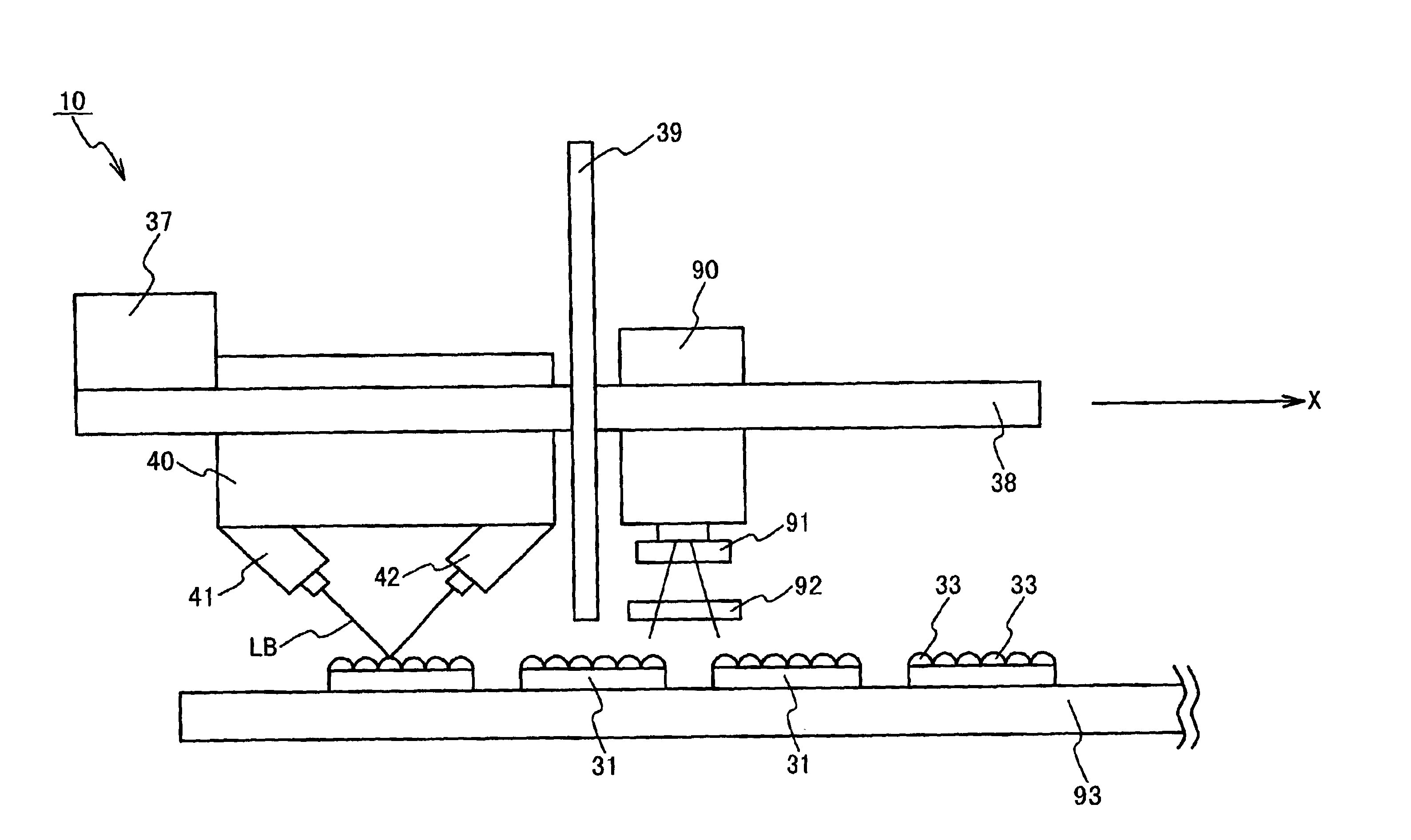
[0083]As shown in FIG. 8, an inspecting apparatus 10 of a semiconductor integrated circuit in this embodiment is used, for example, for inspecting solder balls (bumps) 33 of a plurality of BGA type IC chips 31 placed on a tray 93.

[0084]The inspecting apparatus 10 of the semiconductor integrated circuit is provided with: a laser sensor 40 for carrying out a three-dimension (3D) measurement; an IC appearance inspection CCD camera sensor 90 for carrying out a two-dimension (2D) measurement; and an XY table (not shown) for shifting the laser sensor 40 and the CCD camera sensor 90 at a high accuracy. The inspecting apparatus 10 has a laser light source 41 and a CCD sensor 42.

[0085]This embodiment is configured such that the XY table is used to shift the laser sensor 40 and the CCD camera sensor 90 and then fix a tray 93 on which the IC chip 31 is placed. Here, instead of this conf...


PUM


Abstract

A semiconductor integrated circuit inspecting apparatus inspecting a terminal provided on a mount surface of a semiconductor integrated circuit includes a light emitter, a photographing unit and an inspector. The light emitter emits a linear light obliquely to the mount surface. The photographing unit photographs the mount surface to which the light is emitted to output a photograph signal. The inspector inspects the terminal in accordance with the photograph signal. The photographing unit has N (N is a positive integer) photographing elements. The photograph signal is outputted respectively only from M (M is a positive integer smaller than the N) photographing elements of the N photographing elements.

Description

BACKGROUND OF THE INVENTION[0001]1. Field of the Invention[0002]The present invention relates to an apparatus for and a method of inspecting a semiconductor integrated circuit.[0003]2. Description of the Related Art[0004]The following technique disclosed in Japanese Patent Publication No.6-103171 is known as a conventional apparatus for inspecting a semiconductor integrated circuit. As shown in FIG. 1, a laser beam 2 emitted by a laser oscillator 1 is inputted through a light collecting lens 3 to a scanner 4. The scanner 4 has a function of converting the collected laser beam into slit light through a cylindrical lens and the like and then deviating the slit light through a galvanomirror and the like. Thus, this apparatus is complex and expensive.[0005]A slit light 5 outputted by the scanner 4 is emitted to a target body 6. This target body 6 is photographed by a CCD camera 7. A picture signal outputted by the CCD camera 7 is converted into a one-bit digital picture signal by an A / D...

Claims


Application Information

Patent Timeline
IPC IPC(8): G01N21/88G01N21/956G01N21/89G01B11/02G01B11/24H01L23/12
CPCG01N21/95684G01N2021/8905G01N2021/95646
Inventor SASAKI, YOSHIHIRONAGAO, MASAHIKO
Owner RENESAS ELECTRONICS CORP
Why Eureka
Try Eureka