System and method for calibration of testing equipment using device photoemission

Inactive Publication Date: 2005-10-18
DCG SYST
View PDF2 Cites 10 Cited by
  • Summary
  • Abstract
  • Description
  • Claims
  • Application Information

AI Technical Summary

Benefits of technology

[0008]The present invention provides a method and a system for accurate characterization and correction of delays caused by elements of a tester. The invention also provides a method and system for accurate characterization of the different delays on the different pins of the test boards and on the DUT fixturing. Other characterizations, such as DC voltage; linearity

Problems solved by technology

For example, avalanche breakdown in insulators cause light emission, and detection of such light emission can point to the locations of failure in the device.
Various emission microscopes

Method used


Image

  • System and method for calibration of testing equipment using device photoemission
  • System and method for calibration of testing equipment using device photoemission
  • System and method for calibration of testing equipment using device photoemission

Examples


Example

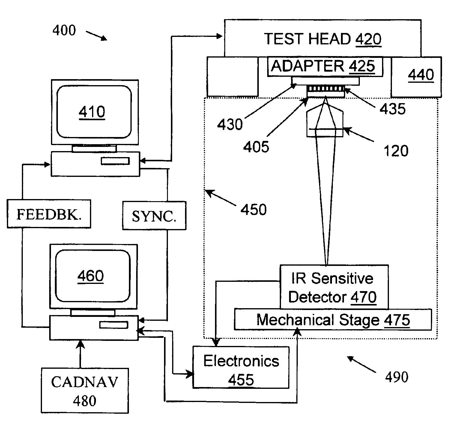
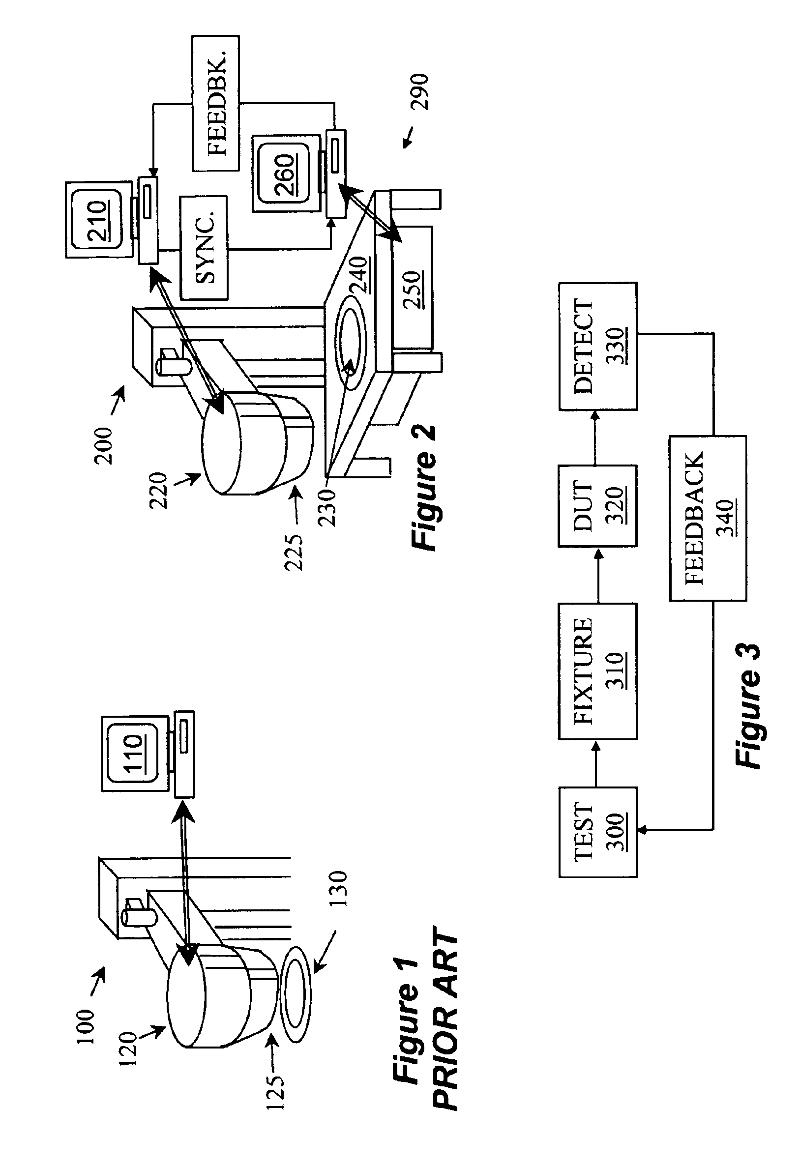
[0025]An illustrative embodiment of the present invention will now be described with reference to FIGS. 2 and 3, which are a general schematic and a block diagram of the inventive calibration system and method, respectively. In FIG. 2, a tester 200 is operable in conjunction with a TRE system 290 such as, e.g., the Emiscope™. The tester comprises, among others, a controller 210, a tester head 220, a DUT adapter 225, and a load board 230. The TRE system 290 comprises, among others, a controller 260 and a detection unit 250, which is mounted onto vibration-isolated bench 240. Both or either of controllers 210 and 260 may be a tailor-programmed general-purpose computer. In performing a typical operation according to the present embodiment, controller 210 emits various test signals that are programmed to stimulate a DUT. The signals are transmitted to the DUT through the various tester intermediate elements, such as the tester head 220, the adapter 225, and the load board 230. This oper...


PUM


Abstract

A system and method for calibration of a commercial semiconductor test system (tester). The system receives a synchronization signal from the tester and detects light emission from a device under test (DUT). The system then compares the timing and characteristics of the light emission to the synchronization signal to obtain a delay timing and signal change caused by intermediate elements of the tester. The delay timing and signal change are used to calibrate the various channels of the tester. Also described are various designs for DUT's to obtained enhanced accuracy of the delay timing. Further, a system and method are described for reconstruction of a test signal and study of the effects of intermediate elements of the tester on the shape of the test signal.

Description

BACKGROUND OF THE INVENTION[0001]1. Field of the Invention[0002]The present invention relates to a method and a system for calibration of semiconductor testing equipment (“tester”) using photoemission detection of switching devices, especially for calibrating signal timing and characteristics in such devices.[0003]2. Description of the Related Art[0004]Testing Equipment (testers) are well known in the art for measuring performance of, and debugging semiconductor circuits. Examples of such equipments are NPTest 9000 available from NPTest of San Jose, Calif., and Vanguard available from IMS (a Credence Company) of Hillsboro, Oreg. FIG. 1 depicts a general schematic of a tester 100, consisting of a controller (may be a tailor-programed general-purpose computer) 110, a test head 120 having a tester load board adapter 125. For debug of an integrated circuit (IC), the IC is attached to a DUT socket (not shown), which is mounted onto the load board 130. The load board 130 is electrically c...

Claims


Application Information

Patent Timeline
IPC IPC(8): G01R31/319G01R31/311G01R31/28G01R31/3193G01R35/00
CPCG01R31/311G01R31/3191G01R35/005G01R31/31937
Inventor NIV, ISRAELKASAPI, STEVEN
Owner DCG SYST
Why Eureka
Try Eureka