Combined content addressable memories

a content addressable memory and combination technology, applied in memory adressing/allocation/relocation, digital storage, instruments, etc., can solve the problems of affecting the response time of methods, affecting the response time of overall content addressable memory, and limited capacity of cam devices

Inactive Publication Date: 2005-10-18
ROBOGROUP TEK
View PDF5 Cites 11 Cited by
  • Summary
  • Abstract
  • Description
  • Claims
  • Application Information

AI Technical Summary

Benefits of technology

[0013]A method and circuit for a high speed interface that enables the integration of several Content Addressable memories into a...

Problems solved by technology

Existing CAM devices have limited capacity, due to the large number of gates necessary to implement them.
However merging many CAMs into a larger Content Addressable Memory requires dedicated interface or connections.
Such interface circuit will in turn cause delays, resulting in a longer response (search) time for the overall Content Addressable Memory.
Various methods have been proposed for cascading CAMs in a modular way (WO99/23662, U.S. Pat. No. 5,930,359), however these methods imply a degradation in response time.
Thus for example in the case of ...

Method used


Image

  • Combined content addressable memories
  • Combined content addressable memories
  • Combined content addressable memories

Examples


Embodiment Construction

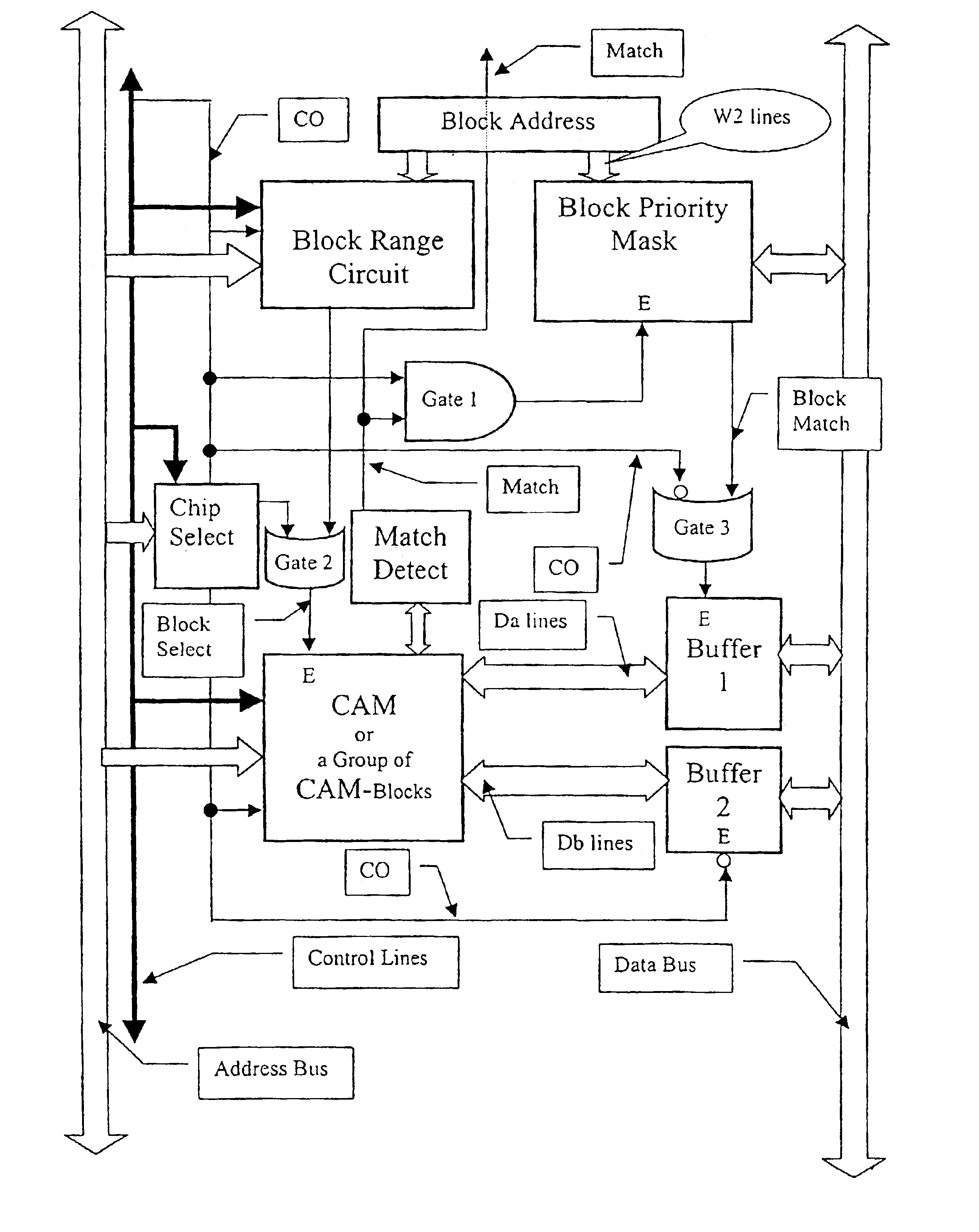
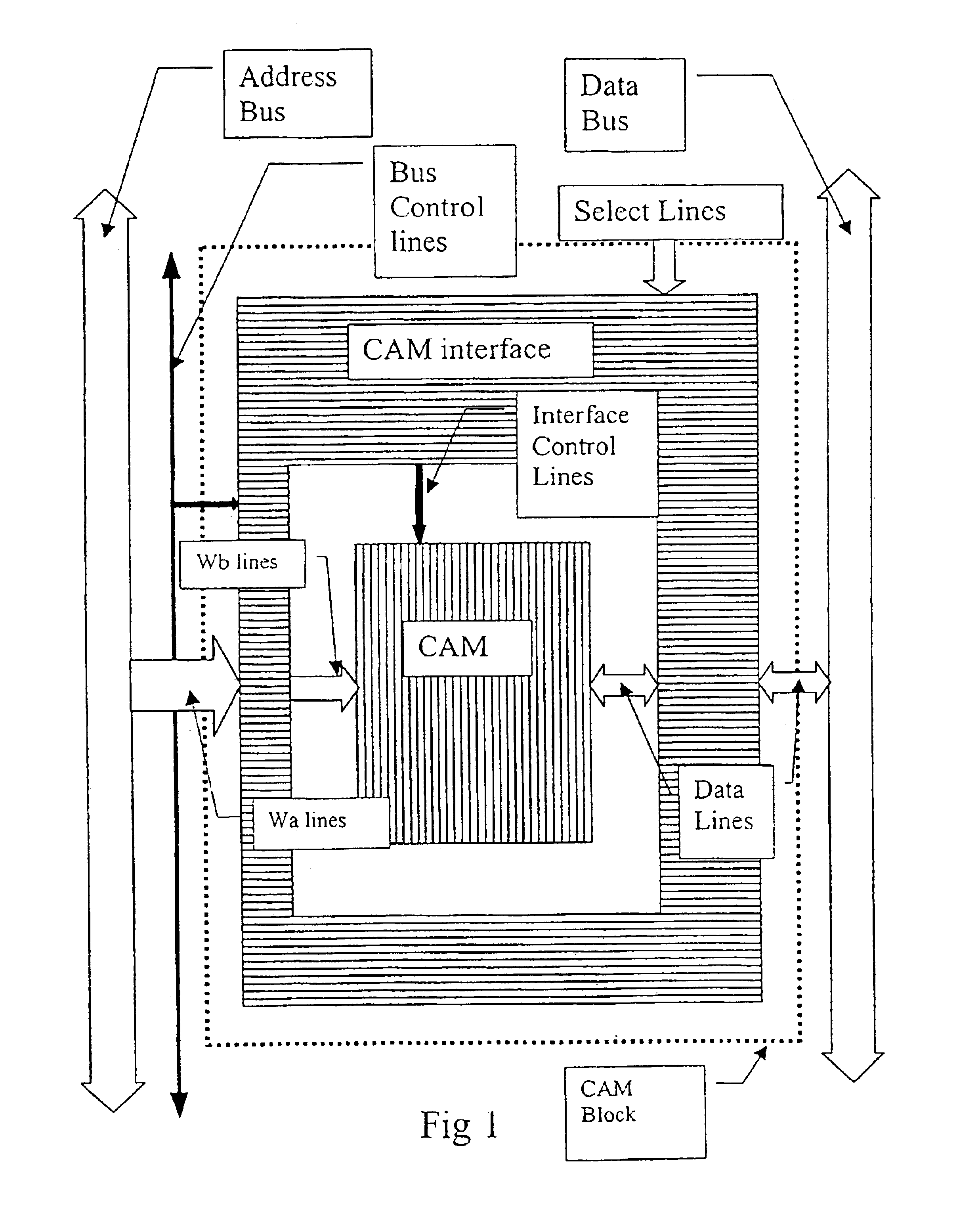
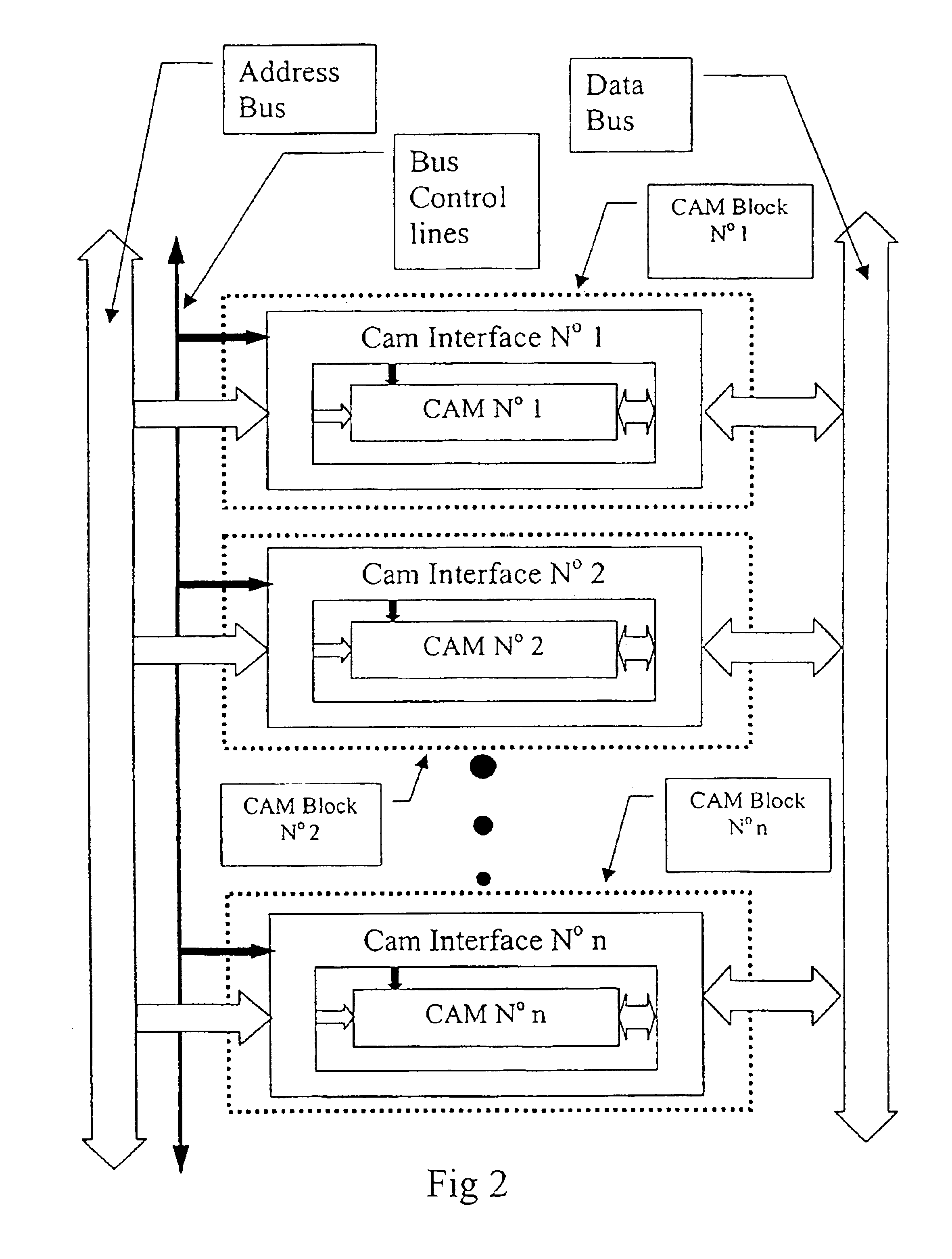
[0023]It is the object of the present invention to provide a high speed interface that enables the integration of several Content Addressable Memories into a larger, Combined Content Addressable Memory. In accordance with the inventive method and circuitry, the new interface provides connections to the BUS system only, and no connection between different CAMs within the same system is needed. The inventive interface is advantageous in that the delay added by the interface is very small, and not dependent on the number of CAMs installed. Thus the novel interface integrates all installed CAMs in one Content Addressable Memory of larger size, having a response time almost equal to that of a single CAM device.

[0024]The inventive interface may also be used to interconnect memories of the Call Out type. These memories are designed to operate in either a R / W mode or a Call Out mode. A Call Out Memory comprises a Range Circuit and when in the Call Out Mode, it will output on the Bus the Add...


PUM


Abstract

A method and circuit for a high speed interface that enables the integration of several Content Addressable memories into a larger, Combined Content Addressable Memory with only an insignificant delay in the original response time of the individual memories. The interface provides connections to the Bus system only and no connection between different CAM devices of the system is needed, whereby the combination of one CAM and one CAM interface in a single device, such as a chip is enabled. Such chips may be used as modules for increasing the CAM Memory by directly attaching them to the Bus System without any additional interface, as known for standard memory chips such as RAM. The inventive interface may also be used for creating a hierarchical structure within a CAM device by dividing the memory cells in groups, each group being interfaced to the larger combined CAM device via an interface according to the invention. In such a structure the priority function in each group operates on a smaller number of cells and due to the relatively small number of gates necessary for making the interface the implementation of a CAM device with a reduced number of gates is facilitated. In a combined CAM device several CAMs are connected to an Address Bus and to a Data Bus via their respective interfaces. In the Read and Write mode, the interface will connect the two sets of lines and thus be transparent for the Read or Write operation. In the search mode (Content Addressing mode), the Interface will select and set a number of lines of the Data Bus according to the CAM response so as to output the address of one matching cell that is the highest in a predefined direction. The interface circuit adds the logic functions and lines necessary to expand the Content addressable functions of the CAM module to a larger range of addresses, sets an additional number of bus lines in order to write the address of the cell within that larger range and checks that no other cell with a higher address responds throughout the system by masking the bits of the CAM address if they would change the address of a cell with a higher address. In this way the whole ensemble of CAMs is capable of functioning as a single CAM of larger size.

Description

FIELD OF THE INVENTION[0001]The present invention relates to a method and circuit for a high-speed interface that enables the integration of several Content Addressable Memories into a larger, Combined Content Addressable Memory.[0002]In the framework of the invention, the term Content Addressable Memory (CAM) will generally refer to a memory device having, in addition to the normal Store and Retrieve functions of a memory, a content addressing function the operation of which may be described as follows:[0003]When a Content Addressable Memory device is placed in the Content Addressing mode, a given value is set on a number of Bus Interface lines, and the device responds by setting on another set of Bus Interface lines data representing the position of one memory cell. That cell, designated hereinbelow the Responding Cell, has stored data verifying a predefined relationship with the data presented on the first Bus Interface Lines (hereinbelow designated Matching Data). In some types ...

Claims


Application Information

Patent Timeline
IPC IPC(8): G11C15/00G11C15/04
CPCG11C15/00
Inventor VILLARET, YVES EMMANUELPROKOPETS, SHMUEL
Owner ROBOGROUP TEK
Why Eureka
Try Eureka