Method of manufacturing trench-type MOSFET

a technology of metal oxide semiconductor and trench-type mosfet, which is applied in the manufacturing of semiconductor/solid-state devices, basic electric elements, electric devices, etc., can solve the problems of non-uniform thickness of trench-type mosfet, and easy to affect punch-through effect of trench-type mosfet devices. , to achieve the effect of uniform thickness and avoiding undes

Inactive Publication Date: 2005-10-25
MOSEL VITELIC INC
View PDF5 Cites 5 Cited by
  • Summary
  • Abstract
  • Description
  • Claims
  • Application Information

AI Technical Summary

Benefits of technology

[0007]The present invention is related to a method of manufacturing MOSFET devices, and particularly to the trench-type MOSFET devices. The present invention is capable of forming bottom oxide layers having uniform thickness on the bottom of the trenches and avoiding undesired damage in the partial semiconductor substrate near the top of the trenches.

Problems solved by technology

However, thinning the gate oxide layer for enhancing the current drive renders the gate oxide layer more easily affected by the punch-through effect.
However, as described above, the trench-type MOSFET device with thinner gate oxide layer is easily affected by the punch-through effect.
In the fabrication of MOSFET devices, because of the arrangements of circuits on the semiconductor substrate, the trenches are not distributed uniformly and formed densely and loosely in different districts on the semiconductor substrate.
The thickness of the bottom-oxide layers of different working devices will also be non-uniform at the bottom of trenches in the subsequent steps.
In another aspect, the etching process performed for forming the bottom-oxide layer also generates undesired damage in the portion of semiconductor substrate near the top of the trench.

Method used


Image

  • Method of manufacturing trench-type MOSFET
  • Method of manufacturing trench-type MOSFET
  • Method of manufacturing trench-type MOSFET

Examples


Embodiment Construction

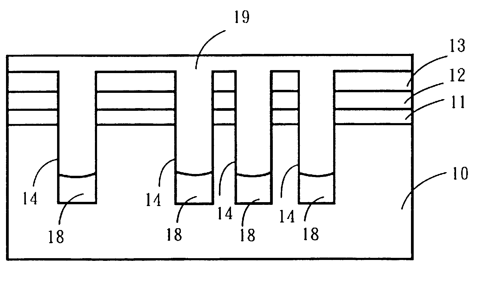
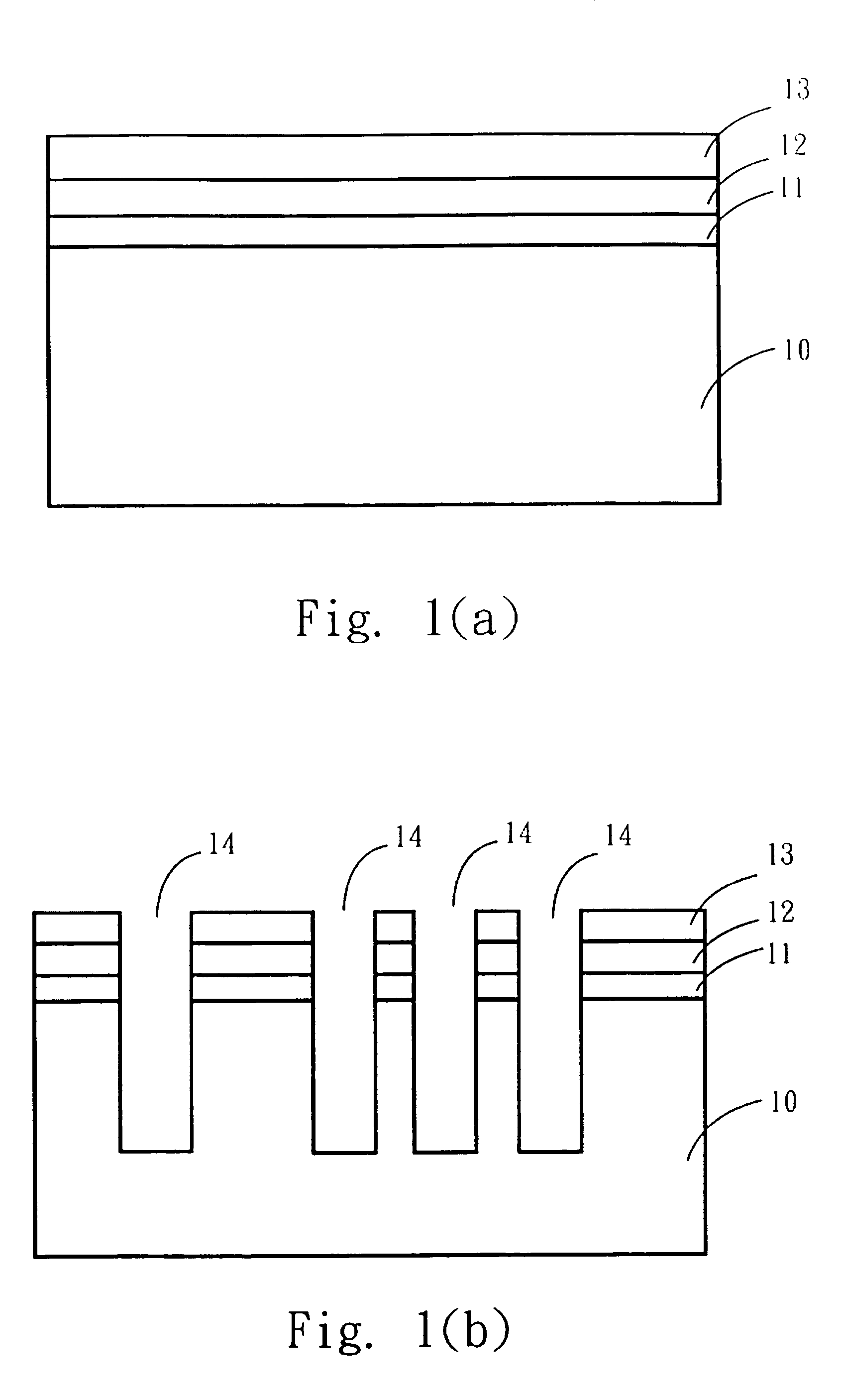
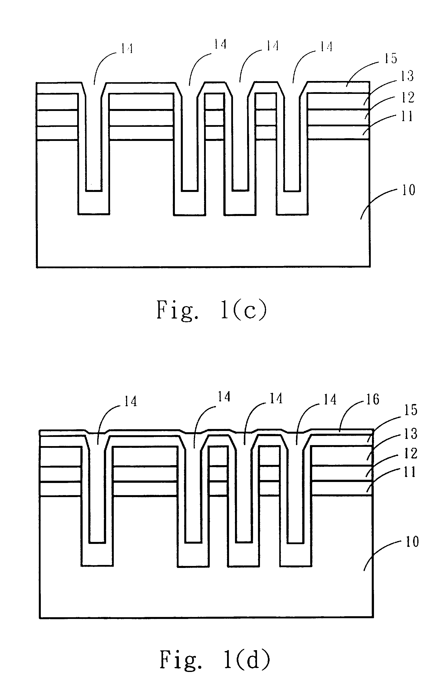
[0012]Embodiments of the present invention provide a method of manufacturing a MOSFET applied to a trench-type MOSFET device. The method prevents the bottom oxide layer from forming non-uniformly and avoids undesired damage near the top of the trench due to the pattern-density distribution of the trenches on the semiconductor substrate. The method also keeps the properties of wafer acceptance test (WAT) from the effect of the traditional disadvantage.

[0013]The present invention will now be described with reference to the following exemplary embodiments. It is to be noted that the following descriptions including device types, dimensions, materials, functionally-equivalent processes or steps do not limit the protective scope of the present invention. The scope of the present invention is defined in the claims.

[0014]FIG. 1(a) to FIG. 1(h) are the schematic cross-sectional views illustrating the process of manufacturing a trench-type MOSFET device according to one embodiment of the pre...


PUM


Abstract

In a method of manufacturing MOSFET devices, and particularly to the trench-type MOSFET devices, embodiments of the present invention provide methods of forming bottom oxide layers having uniform thickness on the bottom of the trenches and avoiding undesired damage in the partial semiconductor substrate near the top of the trenches. In one embodiment, a method for manufacturing a trench-type MOSFET comprises providing a semiconductor substrate and forming a trench on the semiconductor substrate; forming a first oxide layer on a bottom and sidewalls of the trench and on the semiconductor substrate; forming a bottom anti-reflective coating (BARC) layer in the trench to cover the first oxide layer; forming a photoresist layer on the bottom anti-reflective coating layer; removing the photoresist layer; removing the bottom anti-reflective coating layer; and removing the first oxide layer on the sidewalls of the trench to form a bottom oxide layer on the bottom of the trench.

Description

CROSS-REFERENCES TO RELATED APPLICATIONS[0001]This application claims priority from R.O.C. Patent Application No. 092127526, filed Oct. 3, 2003, the entire disclosure of which is incorporated herein by reference.BACKGROUND OF THE INVENTION[0002]The present invention relates to a method of manufacturing a Metal-Oxide Semiconductor Field Effect Transistor (MOSFET) device, and more particularly to a method of manufacturing a trench-type Metal-Oxide Semiconductor Field Effect Transistor (MOSFET) device.[0003]Nowadays, trench-type MOSFET devices are broadly used in the semiconductor industry. The difference between the trench-type MOSFET device and the traditional MOSFET device is that the gate structure of the former is formed in the trench for minimizing the area of the MOSFET device, enhancing the density of the MOSFET device and preventing the on-resistance from increasing rapidly in a short time. However, thinning the gate oxide layer for enhancing the current drive renders the gate...

Claims


Application Information

Patent Timeline
Patent Type & Authority Patents(United States)
IPC IPC(8): H01L21/70H01L21/8234
CPCH01L21/823462H01L21/823487
Inventor LIN, CHEN TANGWU, MING FENGYEH, CHUNG CHIHCHIU, HSIN YEN
Owner MOSEL VITELIC INC
Why Eureka
Try Eureka