Semiconductor memory pipeline buffer

a technology of memory pipeline and memory buffer, which is applied in the field of memory pipeline, can solve the problems of large area, large processing overhead, and large size of the device, and achieve the effect of reducing the access time reducing the effective access speed of the cache memory, and negligible area and processing overhead

Inactive Publication Date: 2005-10-25
HITACHI LTD
View PDF4 Cites 46 Cited by
  • Summary
  • Abstract
  • Description
  • Claims
  • Application Information

AI Technical Summary

Benefits of technology

[0011]According to at least one preferred embodiment of the present invention, a memory is provided comprising a plurality of memory cells, each containing a gain cell structure. Furthermore, the present invention comprises a method of data access in which data is read from the cell array and written to the cell array simultaneously. In this manner, the read and write phases of the destructive write cycle of a gain cell can be overlapped, or pipelined, for consecutive accesses. This leads to an overall increase in the effective access speed of the cache memory. In addition, the circuitry to enable this method is located at each memory bank and requires minimal external control, presenting a solution to the slow access cycle of a gain cell memory with negligible area and processing overhead.
[0012]The data write method presented in at least one of the preferred embodiments is distinct from the conventional case due to the insertion of a data latch between the sense amplifier and the write data line. A write cycle proceeds similar to the conventional case by first conducting a read phase in which the old row data is read into the sense amplifiers. As the signals develop, the new data replaces the old data in the selected columns and the combined data is stored in the latches connected to the sense amplifier. The write phase occurs when the data stored in the latches is presented to the write data line and the write word line is activated, transferring the new data to the cells. An important point of the present invention is that as the write data line is activated and data is written to the cells in the write phase, the read phase of the following read- or write-cycle can proceed simultaneously. This is because the data stored in the latch can be applied to the write data line while the sense amplifier is used to discriminate the data on the read data line. Once the write phase is complete, the data from the next accessed row stored in the sense amplifier is stored in the latch and the cycle can repeat. This pipeline write presents an effective access time to the CPU the same length as the read or write phase, whichever is longer, greatly reducing the access time of the cache memory.

Problems solved by technology

However, as cache memory capacity requirements greatly increase to accommodate for multimedia processing, the large cell size of the 6T SRAM leads to a large area, high cost cache memory solution.
This technology has several drawbacks and faces serious complications as device dimensions are scaled smaller.
Therefore, complex capacitor structures and expensive materials must be used to build a device with adequate capacitance, which leads to expensive fabrication and incompatibilities with standard logic processes.
However, these often fail to be used in products because of a slower access time than SRAM.
This long read then write cycle is a serious detriment to gain cell solutions, especially those with a longer write phase.
Although it is efficient to use this technology in writing a lot of bits of data, it is difficult to adopt this technology in writing small bits of data, for example 8 bit data.
Therefore the feature of 3T memory cell that is high density is damaged.

Method used


Image

  • Semiconductor memory pipeline buffer
  • Semiconductor memory pipeline buffer
  • Semiconductor memory pipeline buffer

Examples


first embodiment

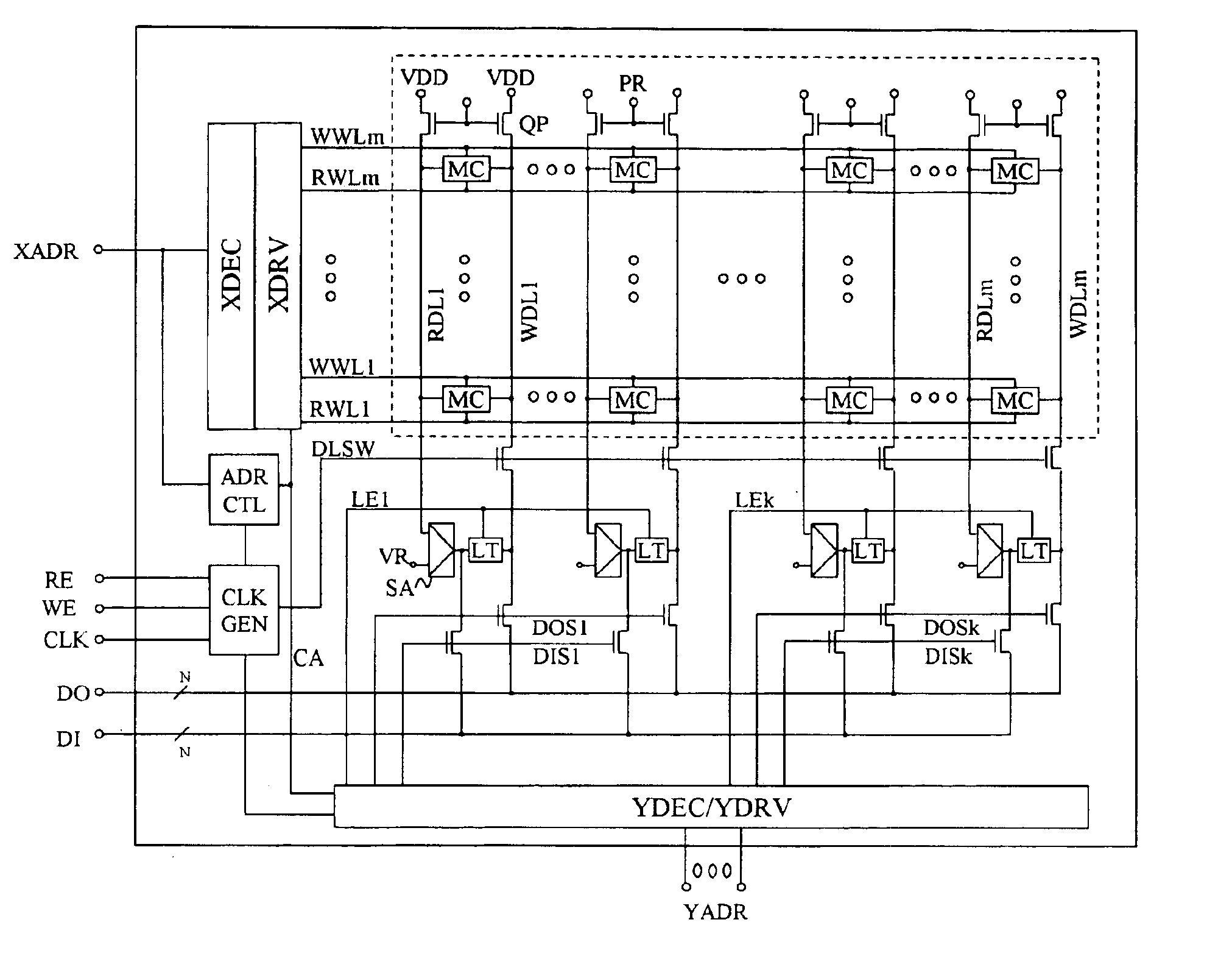
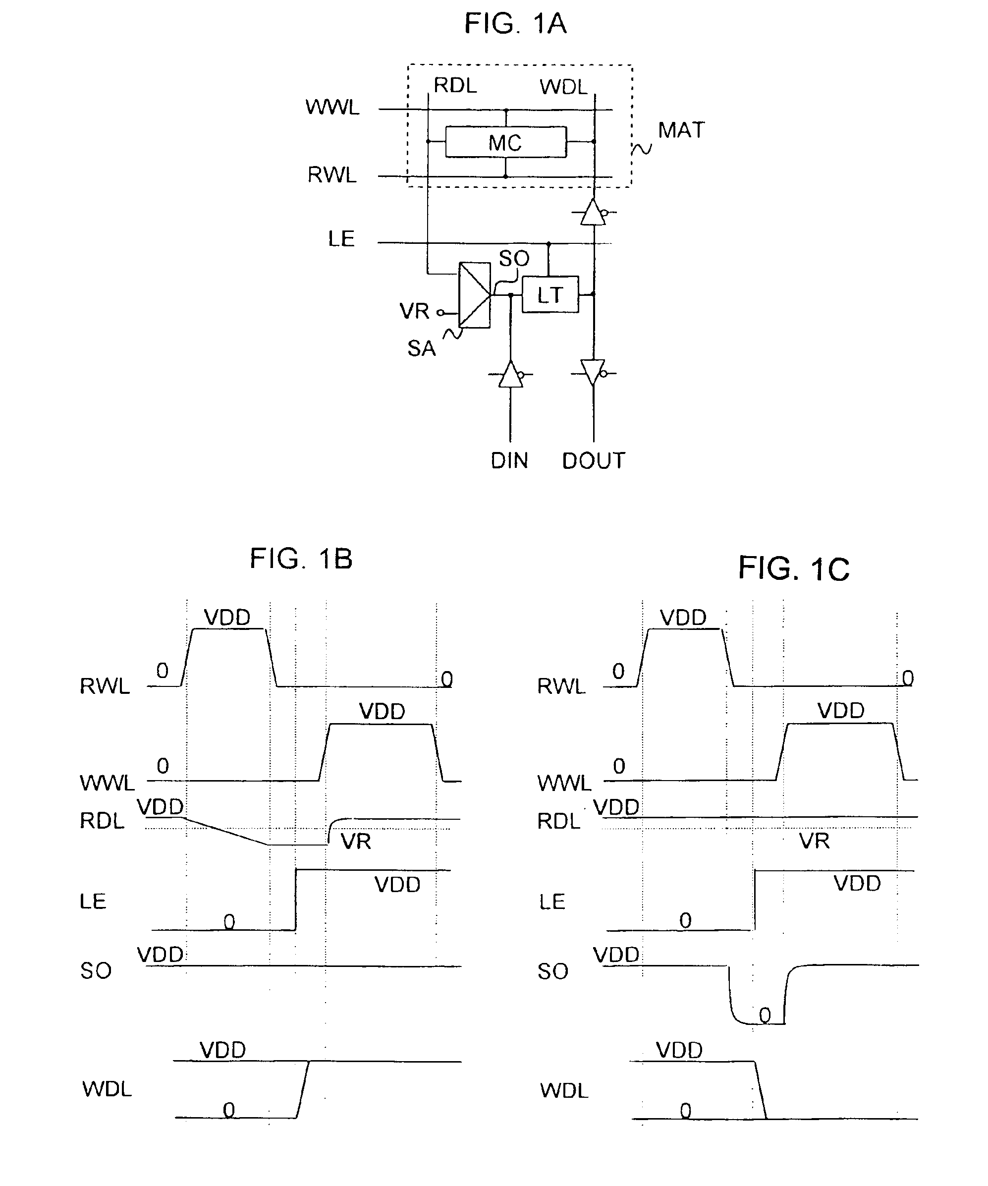
[0038]FIG. 1A is a circuit diagram of a memory circuit, in accordance with the present invention. The block consists of a mat MAT of memory cells arranged in columns and rows and a single memory cell MC is accessed by a read word line RWL, a write word line WWL, a read data line RDL, and a write data line WDL. A sense amplifier SA discriminates the data on the read data line by comparing the signal with a reference signal VR. The output SO of the sense amplifier is connected to the input of a latch element LT. In addition, input data line DIN for the column is also connected to the input of the latch element through a switch element. The output of the latch is connected to the write data line WDL through a switch and presents the write data to the accessed cell. Furthermore, the output of the latch is connected to the data out line DOUT through a buffer used to output read data to the microprocessor.

[0039]Before the access characteristics of this memory architecture are presented, a...

second embodiment

[0060]the present invention presents a structure similar to the first embodiment in which two separate memory mats share a single sense amplifier SA and latch circuit LT.

[0061]FIG. 10A shows the circuit diagram of a pair of array columns and the common sense amplifier and latch circuits, in accordance with the second embodiment of the present invention.

[0062]FIG. 10B shows exemplary access waveforms for the circuitry of FIG. 10A, in accordance with the second embodiment of the present invention. In the second embodiment, the memory is composed of a set of upper memory mats UMAT and lower memory mats LMAT. The cells are controlled by row signals including the read word lines URWL, LRWL and the write word lines UWWL, LWWL. In addition, the mats are divided into columns of cells that are accessed through read data lines URDL, LRDL and write data lines UWDL, LWDL. In this embodiment, the upper read data line URDL and lower write data line LRDL are connected to a single sense amplifier S...

third embodiment

[0065]the present invention concerns memory arrays in which the read phase is much shorter than the write phase of the write cycle.

[0066]FIG. 11A shows the circuit diagram of a single array column, in accordance with the third embodiment of the present invention.

[0067]FIG. 11B shows exemplary access waveforms for the circuitry of FIG. 11A, in accordance with the third embodiment of the present invention. A fundamental difference here from the first embodiment is that several latches are placed between the sense amplifier SA and the write data line WDL instead of a single latch. With this configuration, the effective write access speed of the memory array can be increased versus that in the first embodiment. For a write phase that is several times slower than the read phase, the access speed of the first embodiment is limited to the speed of the write phase. In this embodiment, the effective access speed is limited to the speed of the faster read phase.

[0068]An analysis of the circui...


PUM


Abstract

A high capacity, fast access dynamic random access memory is provided. Furthermore, a pipelined write method can be realized at each array block by affixing a latch between the sense amplifier and write data line for each column. In this manner, a data write phase can occur simultaneously with the pre-read phase of the following address. Using this method, the effective access speed to the array block can be increased, yielding a fast access cache memory.

Description

RELATED APPLICATION[0001]The present application is related to U.S. patent application Ser. No. 10 / 167,754, entitled “Semiconductor Memories”, by inventors Bryan Atwood, Kazuo Yano, Tomoyuki Ishii, Taro Osabe, Kazumasa Yanagisawa, and Takeshi Sakata, filed Jun. 11, 2002, which is hereby incorporated by reference in its entirety.BACKGROUND OF THE INVENTION[0002]1. Field of the Invention[0003]The present invention generally relates to semiconductor memories and, more particularly, to a series of array structures, arrangements, and activation schemes for high density, fast access semiconductor memories that have a separate read and write data line and that exhibit destructive write behavior.[0004]2. Discussion of Background[0005]In conventional microprocessors, a cache memory module is fabricated on the same semiconductor die as the processing logic in order to accommodate rapid data and instruction storage and retrieval. Semiconductor memories for on-chip cache applications are typica...

Claims


Application Information

Patent Timeline
Patent Type & Authority Patents(United States)
IPC IPC(8): G11C11/401G11C11/405G11C11/403H01L21/70H01L21/8242H01L27/108H01L27/10G11C7/10G11C7/22G11C11/4093
CPCG11C7/1039G11C7/1042G11C7/1051G11C7/106G11C7/1078G11C7/1087G11C7/22G11C11/405G11C11/4093G11C2207/2281G11C2207/229H01L27/10885H01L27/10888H10B12/482H10B12/485
Inventor ATWOOD, BRYANWATANABE, TAKAOSAKATA, TAKESHI
Owner HITACHI LTD
Why Eureka
Try Eureka