Current drive system

Inactive Publication Date: 2005-10-25
PANASONIC CORP
View PDF12 Cites 23 Cited by
  • Summary
  • Abstract
  • Description
  • Claims
  • Application Information

AI Technical Summary

Benefits of technology

[0025]It is therefore an object of the present invention to provide a current drive system which is used for driving a display panel and avoids display

Problems solved by technology

In particular, a current drive system for an organic EL panel drives display element circuits by a

Method used


Image

  • Current drive system
  • Current drive system
  • Current drive system

Examples


embodiment 1

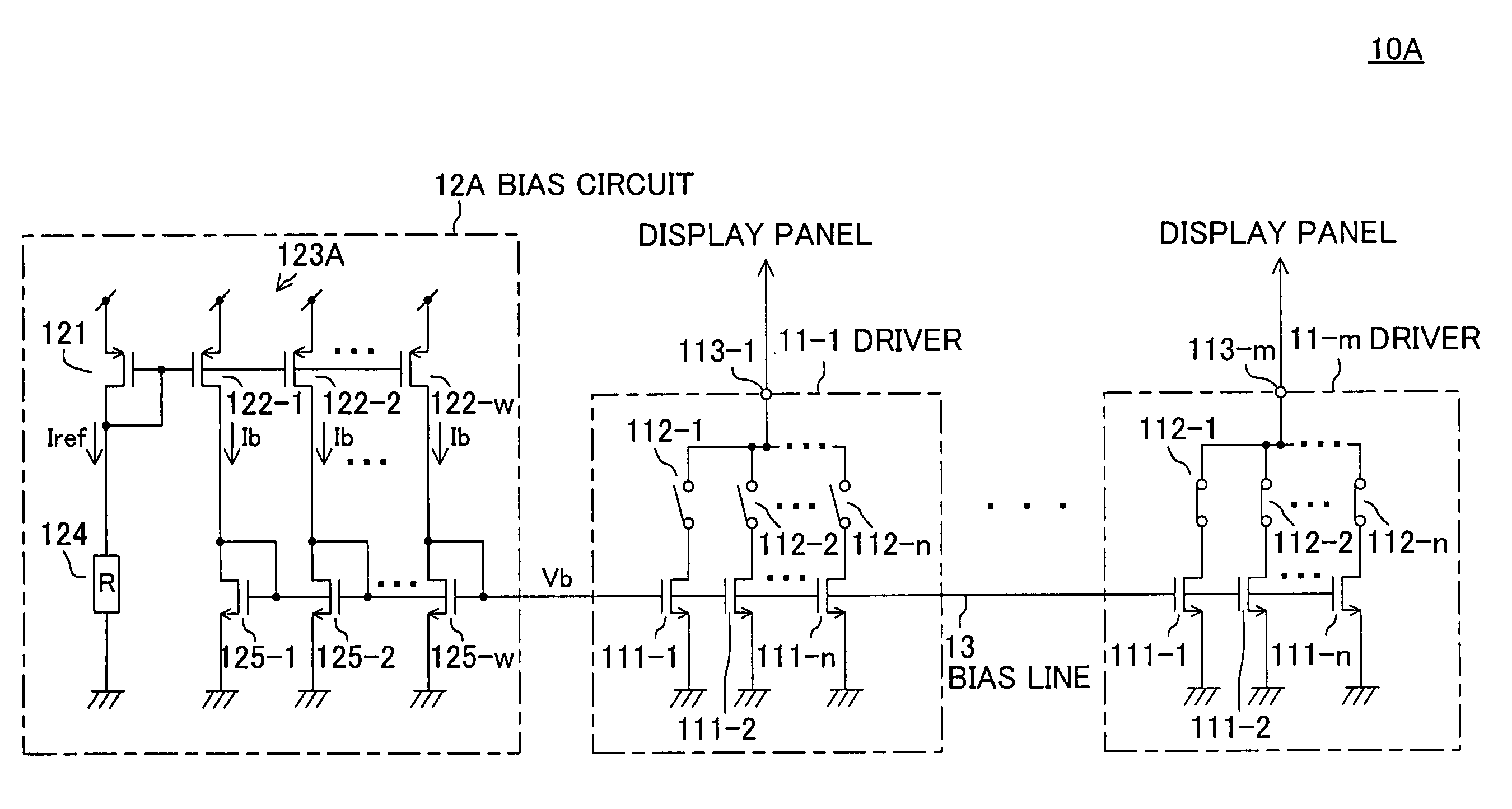
[0059]FIG. 1 shows a circuit configuration of a current drive system according to a first embodiment of the present invention. A current drive system 10A according to this embodiment includes: m drivers 11-1 to 11-m for driving a display panel; and a bias circuit 12A for generating a bias voltage Vb and supplying the bias voltage Vb to each driver 11-i. The driver 11-i is the same as that described in the conventional system, and thus the description thereof will be omitted. Hereinafter, the bias circuit 12A will be described.

[0060]The bias circuit 12A includes: a current mirror circuit 123A including a p-type transistor 121 at its input side and w p-type transistors 122-1 to 122-w connected in parallel at its output side; a resistor 124 connected to the p-type transistor 121 and allowing a reference current Iref to flow at the input side of the current mirror circuit 123A; and w n-type transistors 125-1 to 125-w as a voltage generator receiving a bias current Ib generated by the p-...

embodiment 2

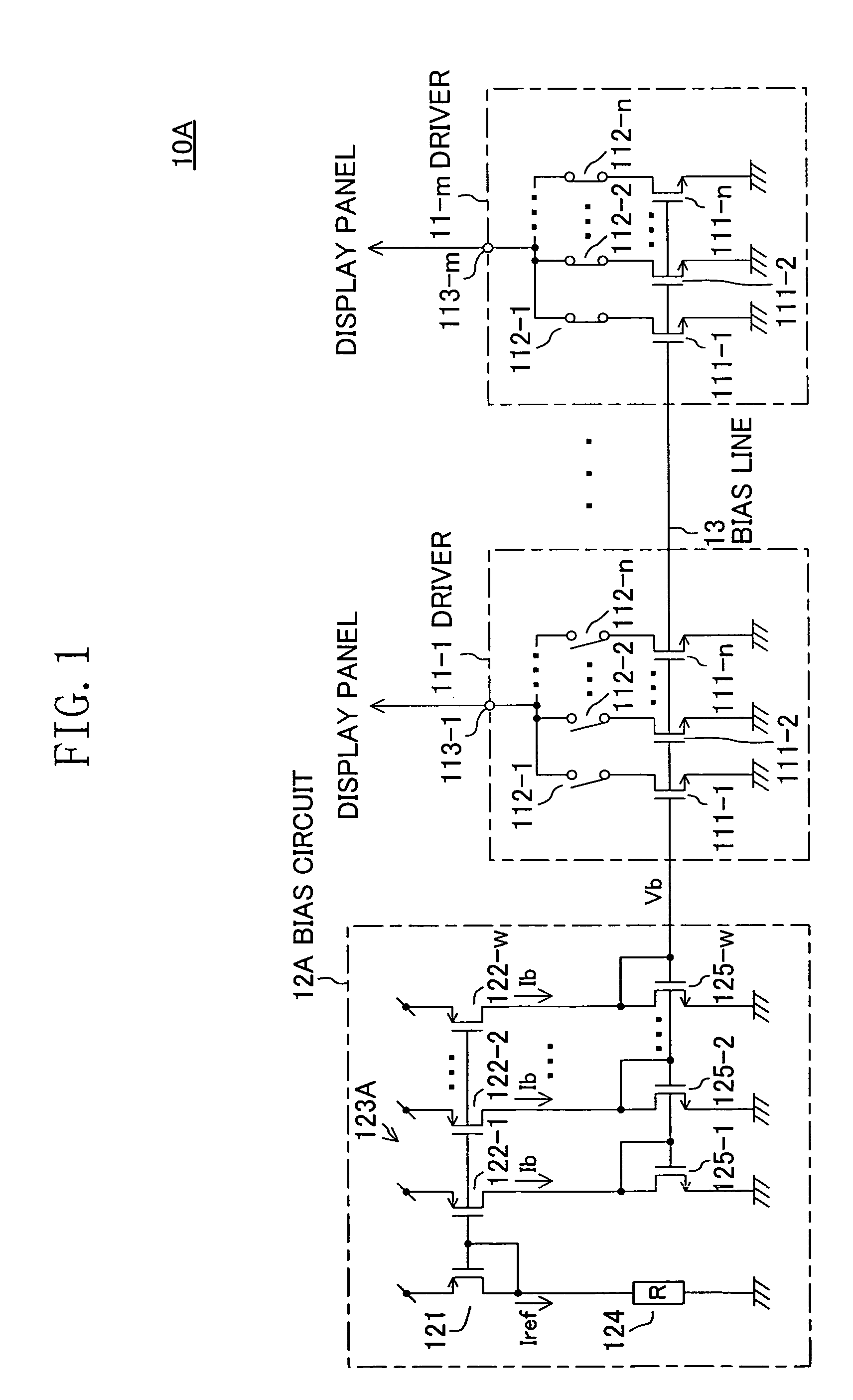
[0063]FIG. 2 shows a circuit configuration of a current drive system according to a second embodiment of the present invention. A current drive system 10B according to this embodiment includes: m drivers 11-1 to 11-m for driving a display panel; and a bias circuit 12B for generating a bias voltage Vb and supplying the bias voltage Vb to each driver 11-i. The driver 11-i is the same as that described in the conventional system, and thus the description thereof will be omitted. Hereinafter, the bias circuit 12B will be described.

[0064]The bias circuit 12B includes: a current mirror circuit 123 having p-type transistors 121 and 122 at its input and output sides, respectively; a resistor 124A connected to the p-type transistor 121 and allowing a reference current Iref to flow at the input side of the current mirror circuit 123; and w n-type transistors 125-1 to 125-w as a voltage generator receiving a bias current generated at the output side of the current mirror circuit 123 to generat...

embodiment 3

[0068]FIG. 3 shows a circuit configuration of a current drive system according to a third embodiment of the present invention. A current drive system 10C according to this embodiment includes: m drivers 11-1 to 11-m for driving a display panel; and a bias circuit 12C for generating a bias voltage Vb and supplying the bias voltage Vb to the driver 11-i. The driver 11-i is the same as that described in the conventional system, and thus the description thereof will be omitted. Hereinafter, the bias circuit 12C will be described.

[0069]The bias circuit 12C has a configuration in which a voltage follower 126 as an impedance reducing means is provided at a subsequent stage in the bias circuit 12 shown in FIG. 10. As well known in the art, the voltage follower 126 has the function of impedance transformation, so that the output impedance of the bias circuit 12C can be set at almost zero. Accordingly, voltage variation, i.e., rising or falling of voltage, caused on a bias line 13 converges w...


PUM


Abstract

In a current drive system for current-driving a display panel such as an organic EL panel, display crosstalk caused by a bias-voltage variation due to induction from the display panel is prevented. For this prevention, the current drive system includes: a plurality of drivers for current-driving a plurality of display element circuits in the display panel; and a bias circuit with a low output impedance for generating a bias voltage and supplying the bias voltage to each of the drivers through a bias line. The output impedance of the bias circuit is set sufficiently low so that a voltage variation caused on the bias line due to switching operation of each switch in the drivers converges within a period during which display data is written.

Description

BACKGROUND OF THE INVENTION[0001]The present invention relates to current drive systems, and particularly relates to techniques with current drive systems suitable as display drivers for organic EL (Electro Luminescence) panels.[0002]In recent years, flat panel displays such as organic EL panels have grown in size and definition and have become thinner, lighter and less expensive. In driving large and high-definition display panels, an active matrix type is preferably chosen in general. Hereinafter, a conventional display driver for an active matrix type display panel will be described.[0003]FIG. 10 shows a circuit configuration of a current drive system as a conventional display driver connected to a display panel. A current drive system 100 includes: m drivers 11-1 to 11-m for current-driving respective display element circuits 21-1 to 21-m in a display panel 20; and a bias circuit 12 for generating a bias voltage Vb and supplying the bias voltage Vb to the driver 11-i (where i is...

Claims


Application Information

Patent Timeline
IPC IPC(8): G05F3/26G05F3/08G09G3/32G09G3/20H01L51/50G09G3/30H03F3/343
CPCG05F3/262G09G3/3283G09G3/3241G09G2320/0209G09G2310/027E01D2/02E01D21/00E01D2101/32
Inventor DATE, YOSHITOOMORI, TETSUROMIZUKI, MAKOTO
Owner PANASONIC CORP
Why Eureka
Try Eureka