Microwave phase shifter having an active layer under the phase shifting line and power amplifier using such a phase shifter

a phase shifter and active layer technology, applied in waveguides, amplifiers, semiconductor devices/discharge tubes, etc., can solve the problems of increasing the number of manufacturing steps, increasing the cost and complicated circuit configuration of the microwave phase shifter formed on the substrate, etc., to achieve easy and precise phase shift adjustment, simple circuit configuration, and easy manufacturing cost reduction

Inactive Publication Date: 2005-11-15
KK TOSHIBA
View PDF9 Cites 15 Cited by
  • Summary
  • Abstract
  • Description
  • Claims
  • Application Information

AI Technical Summary

Benefits of technology

[0010]An object of this invention is to provide a microwave phase shifter in which the circuit configuration is simple and can be easily made small, and as a result, the manufacturing cost can be lowered, and which can relatively easily and precisely adjust a phase shift amount, and a power synthesizing type of power amplifier using the microwave phase shifter.

Problems solved by technology

As a result, the circuit configuration of the microwave phase shifter formed on the substrate becomes complicated, the substrate becomes larger and the cost rises due to an increase in the number of manufacturing steps.
In a power amplifier using this semiconductor amplifier element, the output power which can be acquired by use of one element is not necessarily sufficient.

Method used


Image

  • Microwave phase shifter having an active layer under the phase shifting line and power amplifier using such a phase shifter
  • Microwave phase shifter having an active layer under the phase shifting line and power amplifier using such a phase shifter
  • Microwave phase shifter having an active layer under the phase shifting line and power amplifier using such a phase shifter

Examples


first embodiment

[0021](First Embodiment)

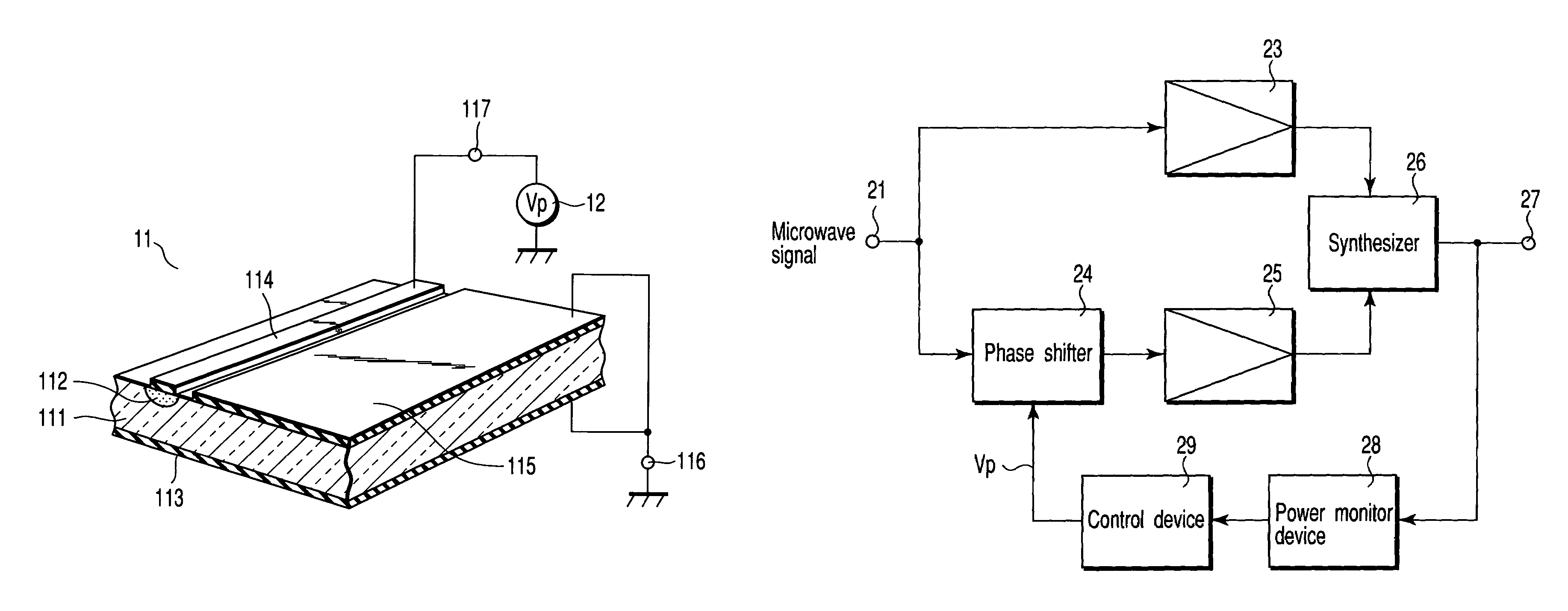
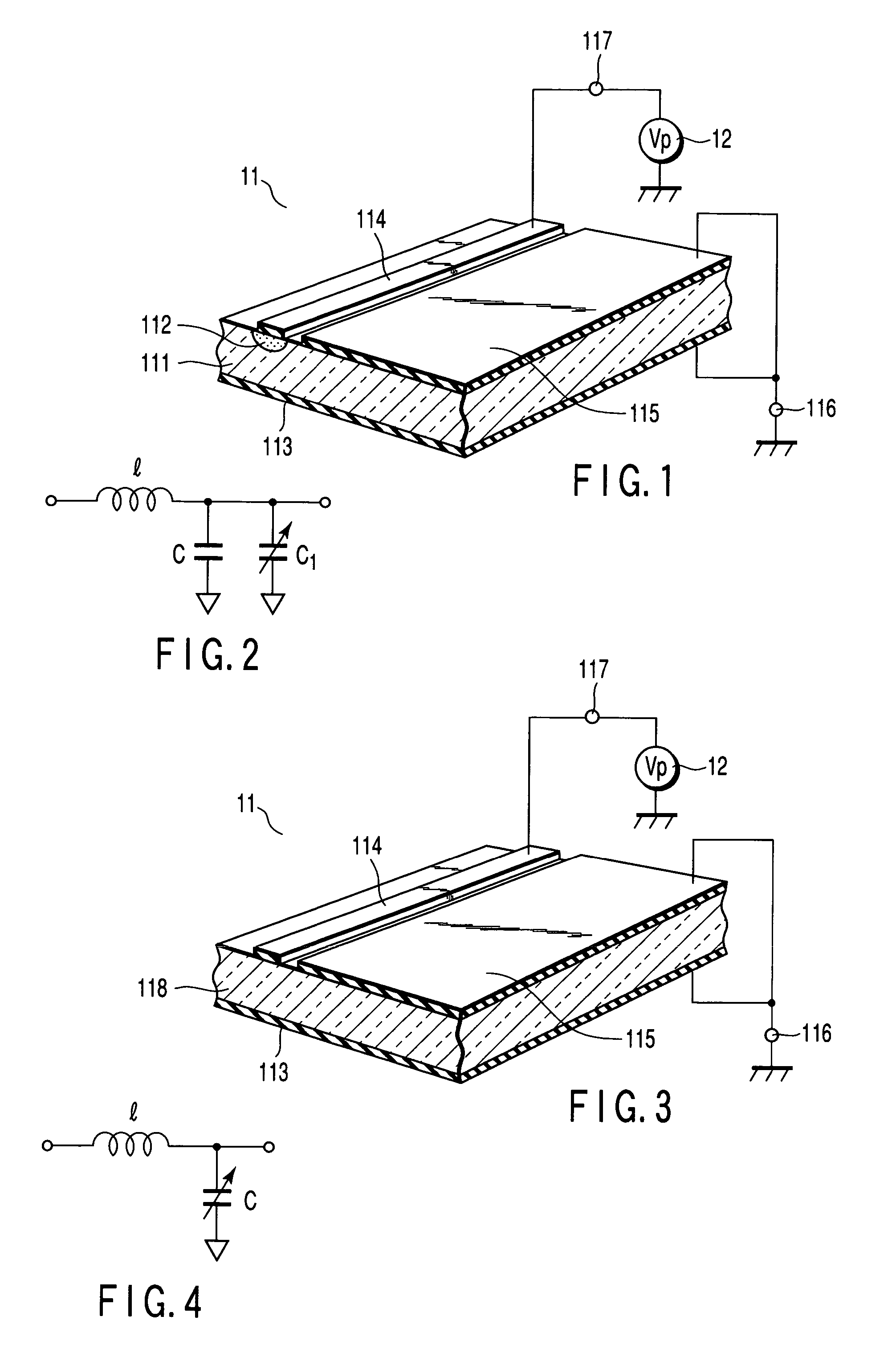
[0022]FIG. 1 is a configuration view showing the configuration of a microwave phase shifter according to a first embodiment of this invention. In FIG. 1, reference label 11 denotes a circuit board of the microwave phase shifter. The circuit board 11 is a semi-insulating substrate having a semi-insulating layer 111 formed of a semi-insulating material such as GaAs. On one surface side (front surface side of the substrate) of the semi-insulating layer 111, an active layer 112 is formed in at least a transmission line forming portion, and on the other surface side (rear surface side of the substrate), a first conductive layer 113 of a metal material is formed. The active layer 112 is formed by ion-implanting an impurity into the semi-insulating layer 111, for example.

[0023]On the upper side of the active layer 112, a transmission line 114 of a metal material is formed. Further, on the surface of the semi-insulating layer 111 on which the transmission line 114 is...

second embodiment

[0032](Second Embodiment)

[0033]FIG. 3 is a configuration view showing the configuration of a microwave phase shifter according to a second embodiment of this invention. In FIG. 3, the same portions as those of FIG. 1 are denoted by the same reference symbols and different portions are taken up and explained here.

[0034]A circuit board 11 shown in FIG. 3 includes a liquid crystal dielectric layer 118 instead of the semi-insulating layer of FIG. 1. Like the first embodiment, a transmission line 114 and first and second grounding conductive layers 113, 115 formed on the front surface and rear surface of the liquid crystal dielectric layer 118 configure a micro-coplanar strip line utilizing the proximity effect.

[0035]However, in the present embodiment, no active layer is formed.

[0036]With the above configuration, if bias voltage Vp is applied to the transmission line 114, voltages are applied to the liquid crystal dielectric layer 118 between the transmission line 114 and the first groun...

third embodiment

[0044](Third Embodiment)

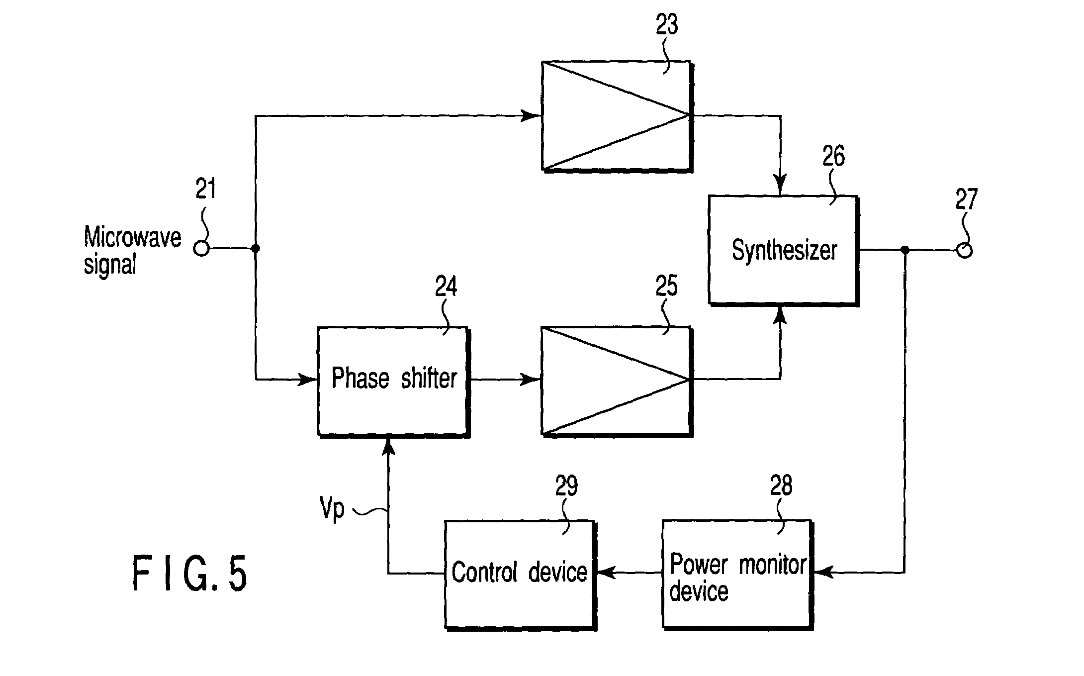
[0045]FIG. 5 is a block circuit diagram showing the configuration of a power amplifier according to a third embodiment of this invention. In FIG. 5, a microwave transmission signal is supplied to an input terminal 21. The signal is distributed into two paths. One of the paths is used as a reference path and the distributed signal thereof is supplied to an amplifier 23 and power-amplified. The distributed signal of the other path is phase-adjusted by a phase shifter 24 so that the phase thereof will correspond to the signal of the reference path and is then supplied to an amplifier 25 and power-amplified. The distributed signals power-amplified by the respective amplifiers 23, 25 are synthesized in a synthesizer 26 and output from an output terminal 27.

[0046]The power amplifier of the above configuration is a so-called power synthesizing type, and it evenly matches the phases when power-amplifying the distributed microwave signals and adds and synthesizes the ...


PUM


Abstract

A phase shifter according to this invention includes a circuit board having a semi-insulating layer. An active layer is formed in a transmission line forming portion on one surface side of the semi-insulating layer, a first ground conductive layer is formed on the other surface side, a transmission line is formed on the upper side of the active layer, and a second ground conductive layer is formed on the transmission line forming surface of the semi-insulating layer in close proximity to one side of the transmission line. If a bias voltage of negative polarity is applied to the transmission line, reverse bias is applied to the active layer to form a depletion layer and capacitance is equivalently connected to the transmission line having inductance. A phase shift amount can be freely controlled by changing the value of the capacitance according to the bias voltage.

Description

CROSS-REFERENCE TO RELATED APPLICATIONS[0001]This is a Continuation Application of PCT Application No. PCT / JP03 / 00852, filed Jan. 29, 2003, which was not published under PCT Article 21(2) in English.[0002]This application is based upon and claims the benefit of priority from the prior Japanese Patent Application No. 2002-023487, filed Jan. 31, 2002, the entire contents of which are incorporated herein by reference.BACKGROUND OF THE INVENTION[0003]1. Field of the Invention[0004]The present invention relates to a microwave phase shifter which gives a desired phase shift amount to a high-frequency signal and a power amplifier using the microwave phase shifter.[0005]2. Description of the Related Art[0006]A microwave phase shifter is a circuit which gives a preset phase shift amount to a high-frequency signal of microwave, millimeter wave or the like and is normally configured by combining several transmission lines, a switch circuit and the like. For example, it has a transmission line ...

Claims


Application Information

Patent Timeline
Patent Type & Authority Patents(United States)
IPC IPC(8): H01P1/18
CPCH01P1/184
Inventor TAKASU, HIDEKI
Owner KK TOSHIBA
Why Eureka
Try Eureka