Active matrix organic electroluminescent display and fabricating method thereof

a technology of active matrix and organic electroluminescent display, which is applied in the direction of discharge tube luminescnet screen, organic semiconductor device, discharge tube/lamp details, etc., can solve the problems of accelerating the degradation of the device, requiring a high drive voltage, and large size of the crt,

Inactive Publication Date: 2005-11-22
LG DISPLAY CO LTD
View PDF7 Cites 18 Cited by
  • Summary
  • Abstract
  • Description
  • Claims
  • Application Information

AI Technical Summary

Benefits of technology

[0017]Another object of the present invention is to provide an organic electroluminescent display device that can be protected from an external impact by forming a thin film transistor and a color changing medium over different substrates and attaching the respective substrates and a fabricating method thereof.

Problems solved by technology

However, a CRT has the disadvantages of being large, heavy, and requiring a high drive voltage.
Because any of the organic electroluminescent layers may break down over the course of time, it may be difficult to maintain the range of all possible colors when the organic electroluminescent display device has been driven for a long period of time.
An increase in the required supply voltage and supply current accelerates the degradation of a device and increases the power consumption of the device.
Although a passive matrix organic electroluminescent display device may be adequate for small display devices, it is not an adequate solution in larger display devices.

Method used


Image

  • Active matrix organic electroluminescent display and fabricating method thereof
  • Active matrix organic electroluminescent display and fabricating method thereof
  • Active matrix organic electroluminescent display and fabricating method thereof

Examples


Embodiment Construction

[0029]Reference will now be made in detail to the preferred embodiments of the present invention, examples of which are illustrated in the accompanying drawings.

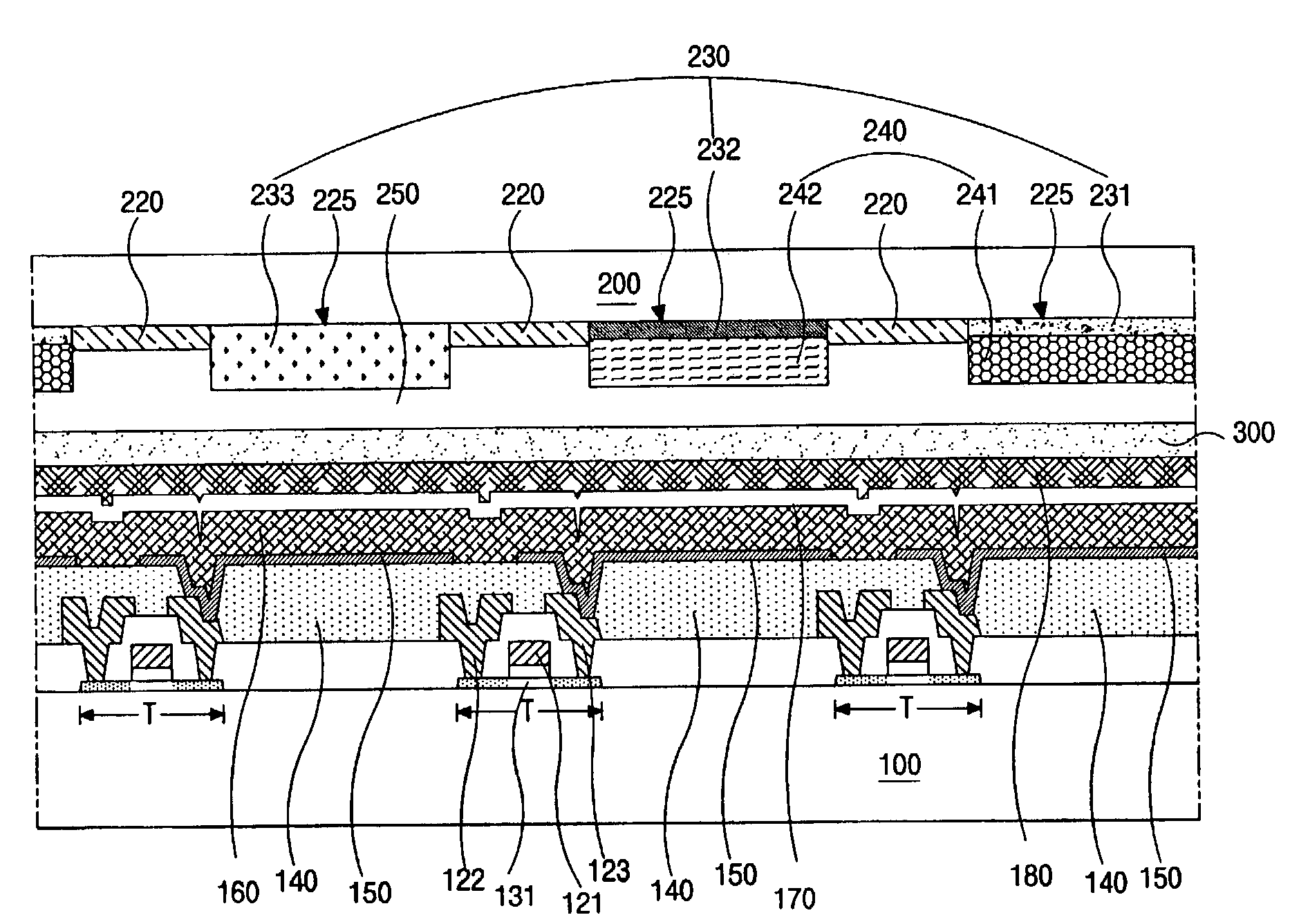
[0030]FIG. 4 is a cross-sectional view of an exemplary organic electroluminescent display device according to the present invention. In FIG. 4, a first substrate 100 and a second substrate 200 may face and be spaced apart from each other. A thin film transistor (TFT) “T” including a gate electrode 121, an active layer 131 of silicon, a source electrode 122, and a drain electrode 123 may be formed on an inner surface of the first substrate 100. A first passivation layer 140 may be formed on the TFT “T.” The first passivation layer 140 may have a drain contact hole exposing the drain electrode 123 and may be composed of either inorganic insulating materials or organic insulating materials. A first electrode 150 of an opaque conductive material may be formed on the first passivation layer 140. An organic electroluminescent laye...


PUM


Abstract

An active matrix organic electroluminescent display device includes a first substrate and a second substrate facing and spaced apart from each other, a thin film transistor on an inner surface of the first substrate, a first electrode connected to the thin film transistor, an organic electroluminescent layer on the first electrode, a second electrode on the organic electroluminescent layer, a passivation layer on the second electrode, a black matrix on an inner surface of the second substrate, the black matrix includes a plurality of open portions, a color filter layer at the plurality of open portions, a color changing layer on the color filter layer, an overcoat layer on the color changing layer, and an adhesive film between the passivation layer and the overcoat layer.

Description

[0001]The present invention claims the benefit of the Korean Patent Application No. P2001-87707 filed in Korea on Dec. 29, 2001, which is hereby incorporated by reference.BACKGROUND OF THE INVENTION[0002]1. Field of the Invention[0003]The present invention relates to an organic electroluminescent display device, and more particularly, to an active matrix organic electroluminescent display device including a thin film transistor and a fabricating method thereof.[0004]2. Discussion of the Related Art[0005]A cathode ray tube (CRT) has been commonly used as a display screen for devices such as televisions and computer monitors. However, a CRT has the disadvantages of being large, heavy, and requiring a high drive voltage. As a result, flat panel displays (FPDs) that are smaller, lighter, and require less power have grown in popularity. Liquid crystal display (LCD) devices, plasma display panel (PDP) devices, field emission display (FED) devices, and electroluminescent display (ELD) devi...

Claims


Application Information

Patent Timeline
Patent Type & Authority Patents(United States)
IPC IPC(8): H01L27/32H01L27/28H01L51/52H01L51/50H05B33/22
CPCH01L27/322H01L27/3244H01L51/524H01L51/5284H01L2251/5315H10K59/38H10K59/12H10K50/841H10K50/865H10K2102/3026H05B33/22
Inventor PARK, JAE-YONGYOO, CHOONG-KEUN
Owner LG DISPLAY CO LTD
Why Eureka
Try Eureka