Voltage regulator combining a series type regulator with a shunt type regulator having a constant current source

a voltage regulator and constant current technology, applied in the direction of electric variable regulation, process and machine control, instruments, etc., can solve the problems of power consumption, power supply current waveform decoding of secret data which should be protected on security,

Inactive Publication Date: 2005-11-22
RAKUTEN GRP INC
View PDF18 Cites 14 Cited by
  • Summary
  • Abstract
  • Description
  • Claims
  • Application Information

AI Technical Summary

Benefits of technology

[0023]According to one aspect of the present invention, there is provided a voltage regulator includes a constant current circuit which is connected between an input node with which a power supply voltage is supplied and an output node to which a load is connected and which supplies constant current to the output node. The voltage regulator also includes a first transistor which is provided in parallel to the constant current circuit and which flows insufficient current to the output node when current flowing through the load is larger than the constant current and a second transis...

Problems solved by technology

However, since current supplied from the power-supply voltage VDD corresponded to load current, there is a problem enable it to analyze operation of the internal logic part of the integrated circuit card, by acting as the monitor of the change of current supplied from the exterior.
When analysis technique, such as DPA/SPA (Differential Power Analysis/Simple Powe...

Method used


Image

  • Voltage regulator combining a series type regulator with a shunt type regulator having a constant current source
  • Voltage regulator combining a series type regulator with a shunt type regulator having a constant current source
  • Voltage regulator combining a series type regulator with a shunt type regulator having a constant current source

Examples


first preferred embodiment

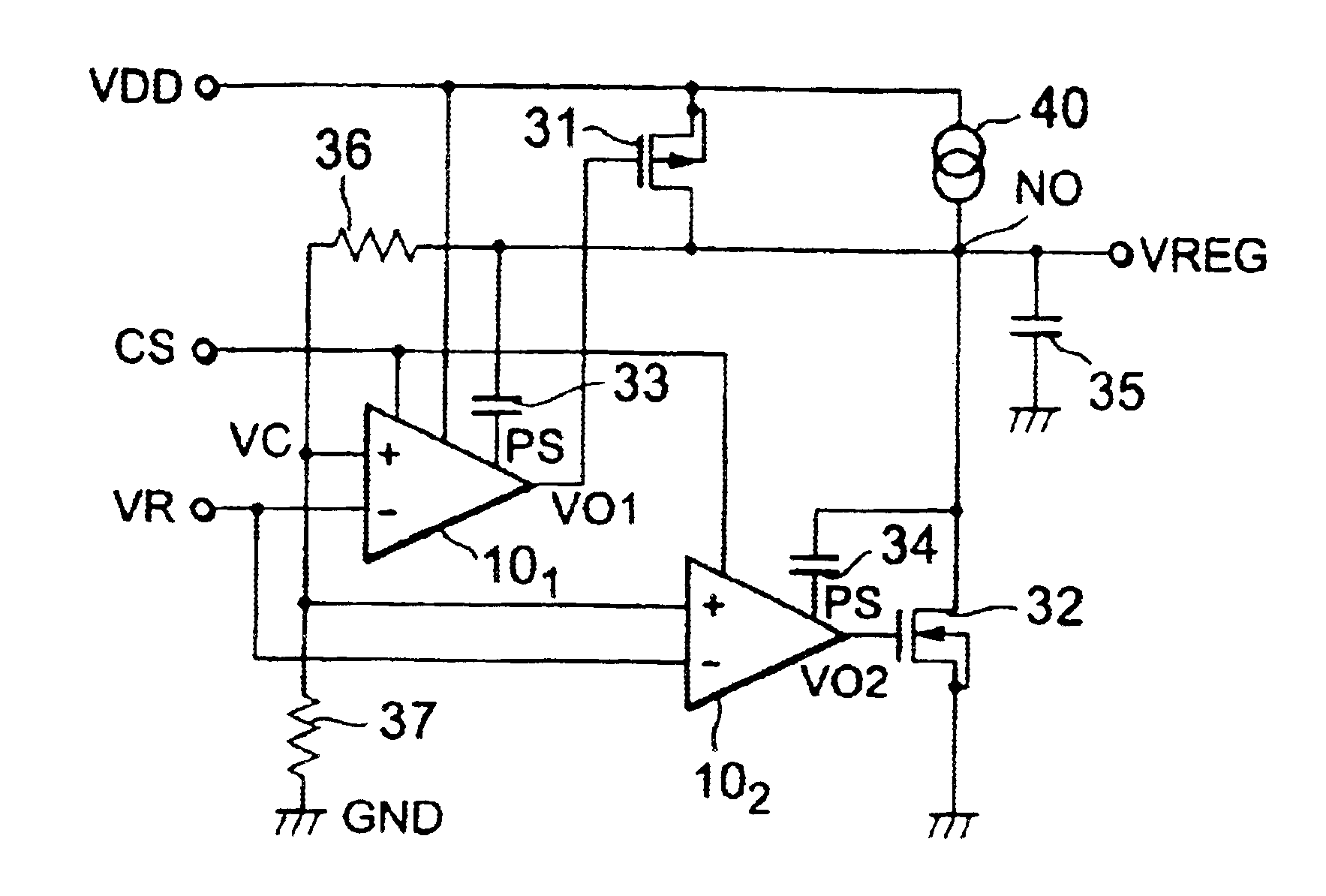
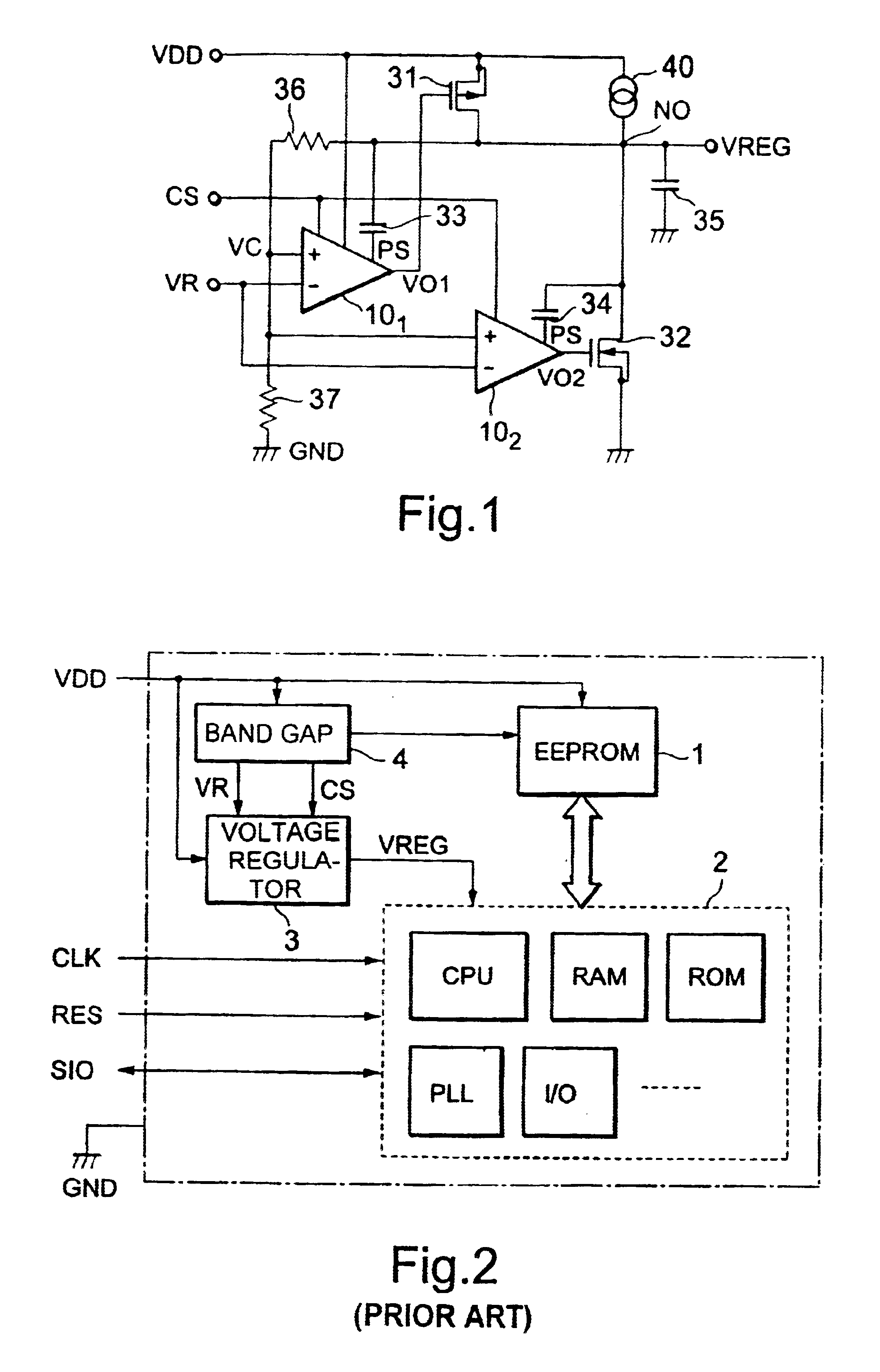
[0035]FIG. 1 is a circuit diagram showing a voltage regulator according to a first preferred embodiment of the present invention.

[0036]This voltage regulator has differential type amplification circuit 101 and amplification circuit 102 where a reference voltage VR is applied to an inverted input terminal −, and a comparison voltage VC is given to an non-inverted input terminal +. The amplification circuit 101 and the amplification circuit 102 are the same structures mutually. The output of the amplification circuit 101 is connected to a gate of a P channel MOS transistor 31 (hereinafter referred to as PMOS) and the output of the amplification circuit 102 is connected to a gate of an N channel MOS transistor 32 (hereinafter referred to as NMOS). A source of the PMOS 31 is supplied with the power-supply voltage VDD and a drain of the PMOS 31 is connected to the output node NO. A drain of the NMOS 32 is connected to the output node NO and a source of the NMOS 32 is connected to a groun...

second preferred embodiment

[0062]FIG. 5 is a circuit diagram showing a voltage regulator according to a second preferred embodiment of the present invention. In FIG. 5, wherein like elements are given like reference characters in FIG. 1.

[0063]The difference between the second embodiment and the first embodiment resides in that a resistor 38 is connected between the resistor 36 and the resistor 37. The sum of resistance value of this resistor 36 and resistance value of the resistor 38 is set as the resistance value of the resistor 36 in FIG. 1. The comparison voltage VC1 appeared at a connection point where the resistor 36 and the resistor 38 are connected to each other may be applied to the non-inverted input terminal + of the amplification circuit 101. The comparison voltage VC2 appeared at a connection point where the resistor 37 and the resistor 38 are connected to each other may be applied to the non-inverted input terminal + of the amplification circuit 102.

[0064]The resistance value of the resistor 38 i...

third preferred embodiment

[0072]FIG. 6 is a circuit diagram showing a voltage regulator according to a third preferred embodiment of the present invention. In FIG. 6, wherein like elements are given like reference characters in FIG. 5.

[0073]This voltage regulator is replaced with the amplification circuit 102 in FIG. 5, and has amplification circuit 10A whose operation is controlled by the control signal S1. Moreover, while a PMOS 51 for a switch by which ON / OFF control is carried out with a control signal S1 is provided between the power-supply voltage VDD and the constant current circuit 40 in series, an NMOS 52 for a switch by which ON / OFF control is carried out with this control signal S1 is provided between the output side of amplification circuit 10A, and the ground potential GND. Other structures are the same as that of FIG. 5.

[0074]FIG. 7 is one example of circuit diagram showing an amplifier circuit 10A in FIG. 6. In FIG. 7, wherein like elements are given like reference characters in FIG. 4(a).

[007...


PUM


Abstract

A voltage regulator includes a constant current circuit which is connected between an input node with which a power supply voltage is supplied and an output node to which a load is connected and which supplies constant current to the output node. The voltage regulator also includes a first transistor which is provided in parallel to the constant current circuit and which flows insufficient current to the output node when current flowing through the load is larger than the constant current and a second transistor which is provided between the output node and a common potential node and which flows surplus current to the common potential node when current flowing through the load is less than the constant current. The voltage regulator also includes a control circuit which controls a conductive state of the first and the second transistors so that an output voltage of the output node is maintained at constant voltage.

Description

REFERENCE TO RELATED APPLICATIONS[0001]This application is a continuing application of application Ser. No. 10 / 207,388, which was filed on Jul. 30, 2002 now U.S. Pat. No. 6,696,822.BACKGROUND OF THE INVENTION[0002]1. Field of the Invention[0003]The present invention generally relates to a voltage regulator used for Integrated Circuit Card and a semiconductor integrated circuit (it is called simply IC hereinafter).[0004]This application relies for priority on Japanese patent application, Serial Number 229374 / 2001, filed Jul. 30, 2001, which is incorporated herein by reference in its entirety.[0005]2. Description of the Related Art[0006]FIG. 2 is a system configuration figure showing an example of an integrated circuit card. This integrated circuit card has the internal logic part 2. This internal logic part 2 has EEPROM 1 (it is a nonvolatile memory which can electrically erase data stored therein), and CPU (Central Processing Unit) and ROM. The EEPROM 1 is a memory for memorizing da...

Claims


Application Information

Patent Timeline
IPC IPC(8): G05F3/24G05F3/26G05F3/08G11C16/06G11C5/14G11C16/30G05F1/618G05F1/56
CPCG05F1/618G05F3/242G05F3/262G11C5/147G11C16/30
Inventor TAKABAYASHI, YASUTAKA
Owner RAKUTEN GRP INC
Why Eureka
Try Eureka