Lowpass filter formed in a multi-layer ceramic

a lowpass filter and multi-layer ceramic technology, applied in the field of elliptic lowpass filters, can solve the problems of requiring additional inductors, requiring additional inductors, and affecting the performance of lowpass filters, so as to reduce the overall area of the lowpass filter, improve the stopband rejection, and reduce the effect of circuit area

Inactive Publication Date: 2005-11-29
CHI MEI COMM SYST INC
View PDF9 Cites 39 Cited by
  • Summary
  • Abstract
  • Description
  • Claims
  • Application Information

AI Technical Summary

Benefits of technology

[0009]It is therefore an objective of the claimed invention to provide a lowpass filter realized with lumped elements in a multi-layered substrate that can provide the response of an elliptic lowpass filter with fewer circuit elements.
[0012]It is an advantage of the claimed invention that the negative mutual inductance introduced between inductors connected to a common node gives the lowpass filter having a structure of a conventional lowpass filter the frequency response of a conventional elliptic lowpass filter. Therefore, an improved stopband rejection is achieved while decreasing the circuit area needed to build the lowpass filter. It is another advantage of the claimed invention that the lowpass filter formed in the multi-layered substrate has a stacked arrangement. The stacked arrangement allows the vertical arrangement of circuit components such that each layer can be built with a small area, thereby decreasing the overall area of the lowpass filter.

Problems solved by technology

Performance of lowpass filters is characterized by insertion losses in the passband and rejections in the stopband.
Although elliptic lowpass filters exhibit much better performance compared to conventional lowpass filters, they require additional inductors.
This is especially undesirable for modern wireless communication devices that are subject to stringent requirements on size and cost.

Method used


Image

  • Lowpass filter formed in a multi-layer ceramic
  • Lowpass filter formed in a multi-layer ceramic
  • Lowpass filter formed in a multi-layer ceramic

Examples


first embodiment

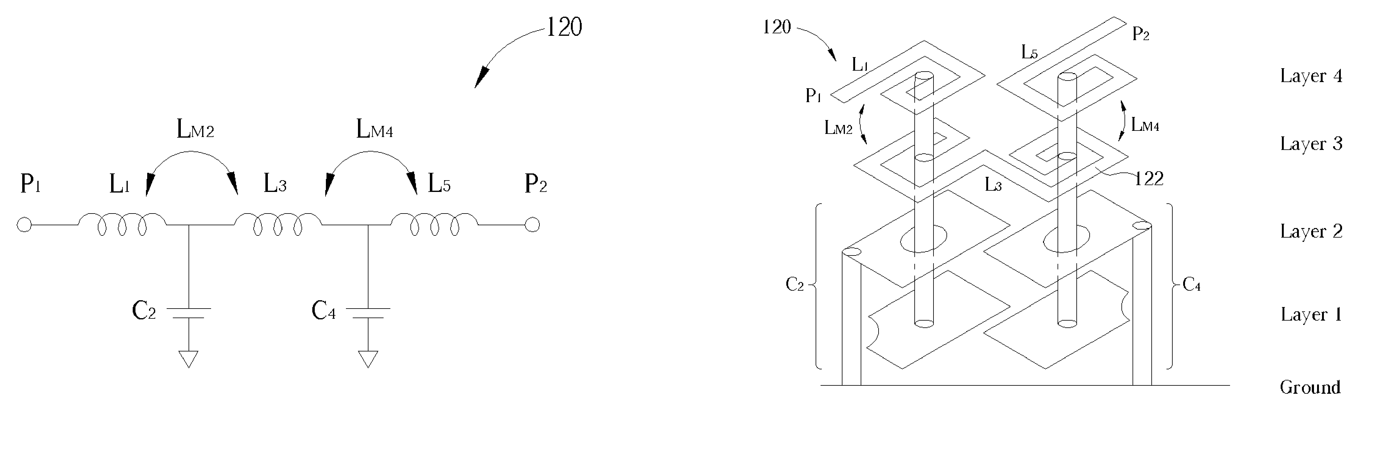
[0038]Please refer to FIG. 6 and FIG. 7. FIG. 6 is a circuit model of a third-order filter 50 according to the present invention. FIG. 7 is a perspective diagram showing the third-order filter 50 realized in a multi-layered substrate with a bottom ground plane according to the present invention. A total of four layers are shown plus the ground plane. On layer 4, inductor L1 is formed out of a spiral inductor 52 that may be made out of a spiral metal strip. One end of the spiral inductor 52 is connected to port P1 and the other end of the spiral inductor 52 is connected to a contact node 54. The contact node 54 connects the spiral inductor 52 to a via 56 that extends from layer 1 to layer 4. On layer 3, inductor L3 is formed out of a spiral inductor 60. The spiral inductor 60 is connected between port P2 at one end and to the via 56 through a contact node 58 at the other end. Capacitor C2 is formed between layer 2 and the ground plane. Layer 2 contains a metal plate 62 with a hole 63...

second embodiment

[0041]Please refer to FIG. 9. FIG. 9 is a perspective diagram of a third-order filter 72 according to the present invention. The third-order filter 72 is similar to the third-order filter 50 of FIG. 7 except the capacitor C2 of the third-order filter 72 is formed on only one layer, which is layer 1. Because the capacitor C2 is formed on only one layer, the third-order filter 72 can be built using one less layer than the third-order filter 50 of FIG. 7.

third embodiment

[0042]Please refer to FIG. 10. FIG. 10 is a perspective diagram showing a third-order filter 80 realized in a multi-layered substrate according to the present invention. The third-order filter 80 is realized in a total of five layers plus the ground plane. Layers 4 and 5 of the third-order filter 80 are exactly the same as layers 3 and 4 of the third-order filter 50 shown in FIG. 7. Instead of using two layers containing metal sheets to form capacitor C2, the third-order filter 80 forms the capacitor C2 out of three layers of metal sheets. On layer 3, a metal sheet 86 connects to a via 82 at contact node 84. The metal sheet 86 connects to another via 90 at contact node 88. The via 90 serves to connect the metal sheet 86 on layer 3 to a metal sheet 100 on layer 1 through contact node 98. Therefore, the metal sheet 86 is electrically connected to the metal sheet 100 for providing a larger effective capacitive area. Another metal sheet 94 is formed on layer 2, and is connected to via 9...


PUM

PropertyMeasurementUnit
mutual inductanceaaaaaaaaaa
frequenciesaaaaaaaaaa
insertion lossesaaaaaaaaaa

Abstract

A lowpass filter formed in a multi-layered substrate includes a first capacitor formed on at least one layer of the multi-layered substrate and being electrically connected to a first node, a first inductor being electrically connected to the first capacitor at the first node, and a second inductor being electrically connected to the first inductor and the first capacitor at the first node. In the lowpass filter, negative mutual inductance exists between the first inductor and the second inductor.

Description

BACKGROUND OF INVENTION[0001]1. Field of the Invention[0002]The present invention relates to a lumped-element elliptic lowpass filter, and more particularly, to a lumped-element elliptic lowpass filter realized in a multi-layered substrate.[0003]2. Description of the Prior Art[0004]Lowpass filters are widely used as building blocks in circuit designs. They are usually used to filter out unwanted spurious responses and harmonics of higher frequencies. Performance of lowpass filters is characterized by insertion losses in the passband and rejections in the stopband.[0005]Please refer to FIG. 1. FIG. 1 is a prototype circuit of a conventional nth-order lowpass filter 10, where n is an odd number. P1 and P2 are two ports of the lowpass filter 10. The lowpass filter 10 contains inductors L1, L3, L5, . . . , Ln and capacitors C2, C4, . . . , Cn-1. For cases in which the rejection in the stopband of the lowpass filter 10 shown in FIG. 1 is not enough to meet system requirements, an ellipti...

Claims


Application Information

Patent Timeline
Patent Type & Authority Patents(United States)
IPC IPC(8): H01F17/00H03H7/01H03H7/09H05K1/03H05K1/16
CPCH03H7/0123H03H7/09H01F2017/0026H03H2001/0085H05K1/0306H05K1/162H05K1/165
Inventor LIN, YO-SHENLI, KO-MAI
Owner CHI MEI COMM SYST INC
Why Eureka
Try Eureka