Semiconductor dynamic quantity sensor with movable electrode and fixed electrode supported by support substrate
- Summary
- Abstract
- Description
- Claims
- Application Information
AI Technical Summary
Benefits of technology
Problems solved by technology
Method used
Image
Examples
first embodiment
[0040](First Embodiment)
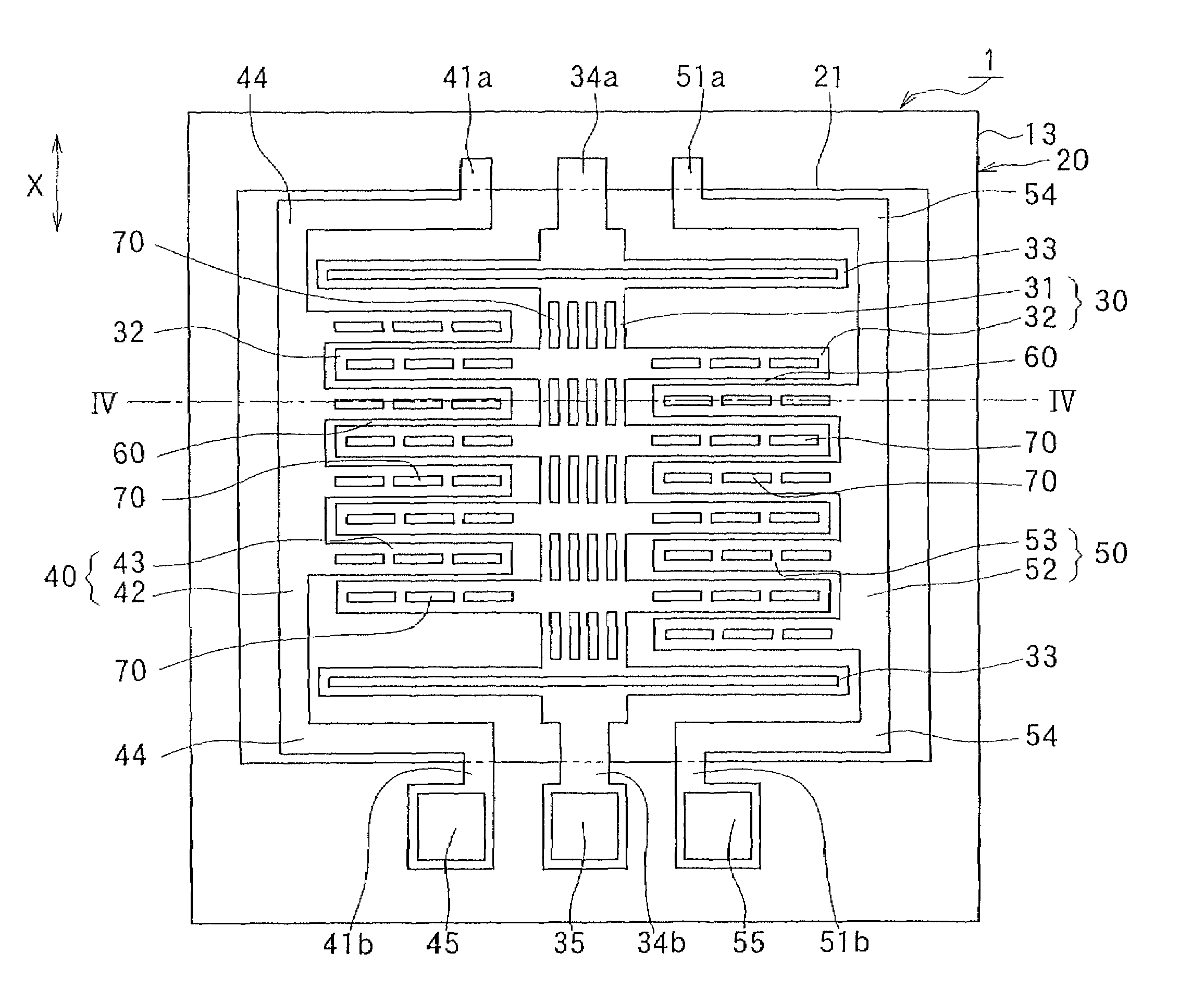
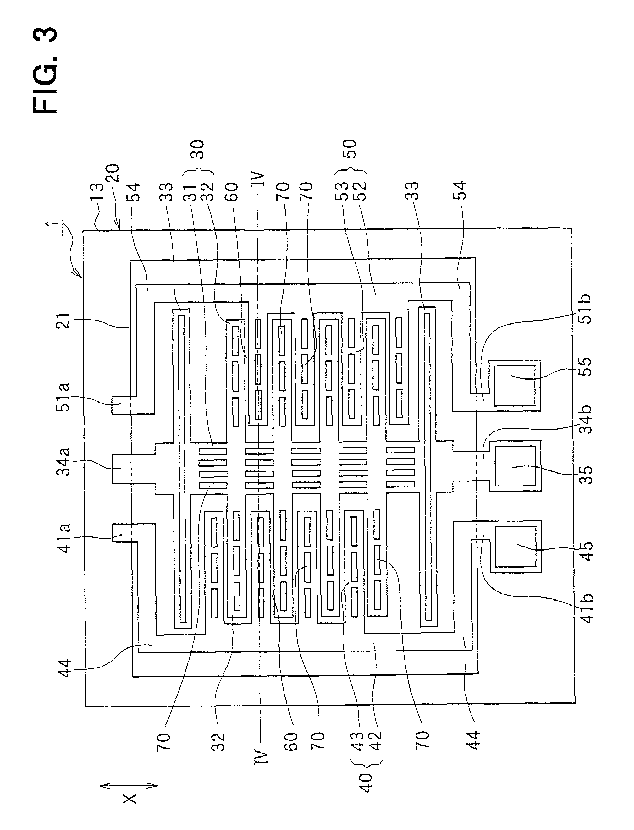
[0041]In a first preferred embodiment, the present invention is applied to a differential capacitance type semiconductor acceleration sensor 1 shown in FIGS. 3 and 4 adopted as a capacitance type dynamic quantity sensor.
[0042]Referring to FIGS. 3 and 4, the sensor 1 is formed by performing micro-machine processing. A semiconductor substrate forming the sensor 1 is, as shown in FIG. 4, an SOI (Silicon On Insulator) substrate 10 that is composed of a first silicon substrate 11 as a first semiconductor layer, a second silicon substrate 12 as a second semiconductor layer, and an oxide film 13 as an insulation layer interposed between the first and second silicon substrates 11 and 12. The first silicon substrate 11 and the oxide film 13 constitute a support substrate 20 in the present invention.
[0043]An opening portion 21 is formed in the support substrate 20 to be open on a surface of the support substrate 20 at a side of the second silicon substrate 21. A beam s...
second embodiment
[0076](Second Embodiment)
[0077]Next, a capacitance type semiconductor acceleration sensor 100 in a second preferred embodiment is explained referring to FIGS. 9A and 9B, which is used for, for example, an air bag system, an ABS system, and the like for vehicles.
[0078]As shown in FIG. 9B, the acceleration sensor 100 is constituted by an SOI substrate 105 that is composed of a first semiconductor layer 103a made of single crystal silicon and having a frame shape with a through hole 102a therein, a second semiconductor layer (SOI layer) 103b made of single crystal silicon for detecting acceleration, and an embedded oxide film 104 provided between the first and second semiconductor layers 103a, 103b. The oxide film 104 is made of SiO2 and has a through hole 102b. The oxide film 104 is a thermally oxidized film having a thermal expansion coefficient approximately equal to that of single crystal silicon forming the semiconductor layers 103a, 103b.
[0079]The second semiconductor layer 103b...
PUM
 Abstract
Description
Claims
Application Information


