Method of forming a semiconductor laser chip having a marker

Active Publication Date: 2005-12-13
NEOPHOTONICS SEMICON GK
View PDF1 Cites 0 Cited by
  • Summary
  • Abstract
  • Description
  • Claims
  • Application Information

AI Technical Summary

Benefits of technology

[0007]The present invention may provide a method for forming a semiconductor chip having chip markers with no flaws and free of the occurrence of deformation and peeling.

Problems solved by technology

Since, however, the markers on the chip are formed on the silicon oxide film, they might produce imperfections that the metal surfaces of the markers are flawed, the shapes thereof are reduced or become large in reverse, or the markers are deformed and peeled as the case may be.
When the imperfections occur in such markers, a problem arises in that the chip cannot be packaged on a mounting board due to passive alignment even if the chip per se is a non-defective item free of any problem in terms of its characteristic.

Method used


Image

  • Method of forming a semiconductor laser chip having a marker
  • Method of forming a semiconductor laser chip having a marker
  • Method of forming a semiconductor laser chip having a marker

Examples


first embodiment

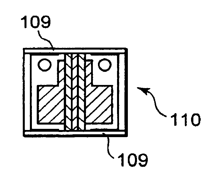
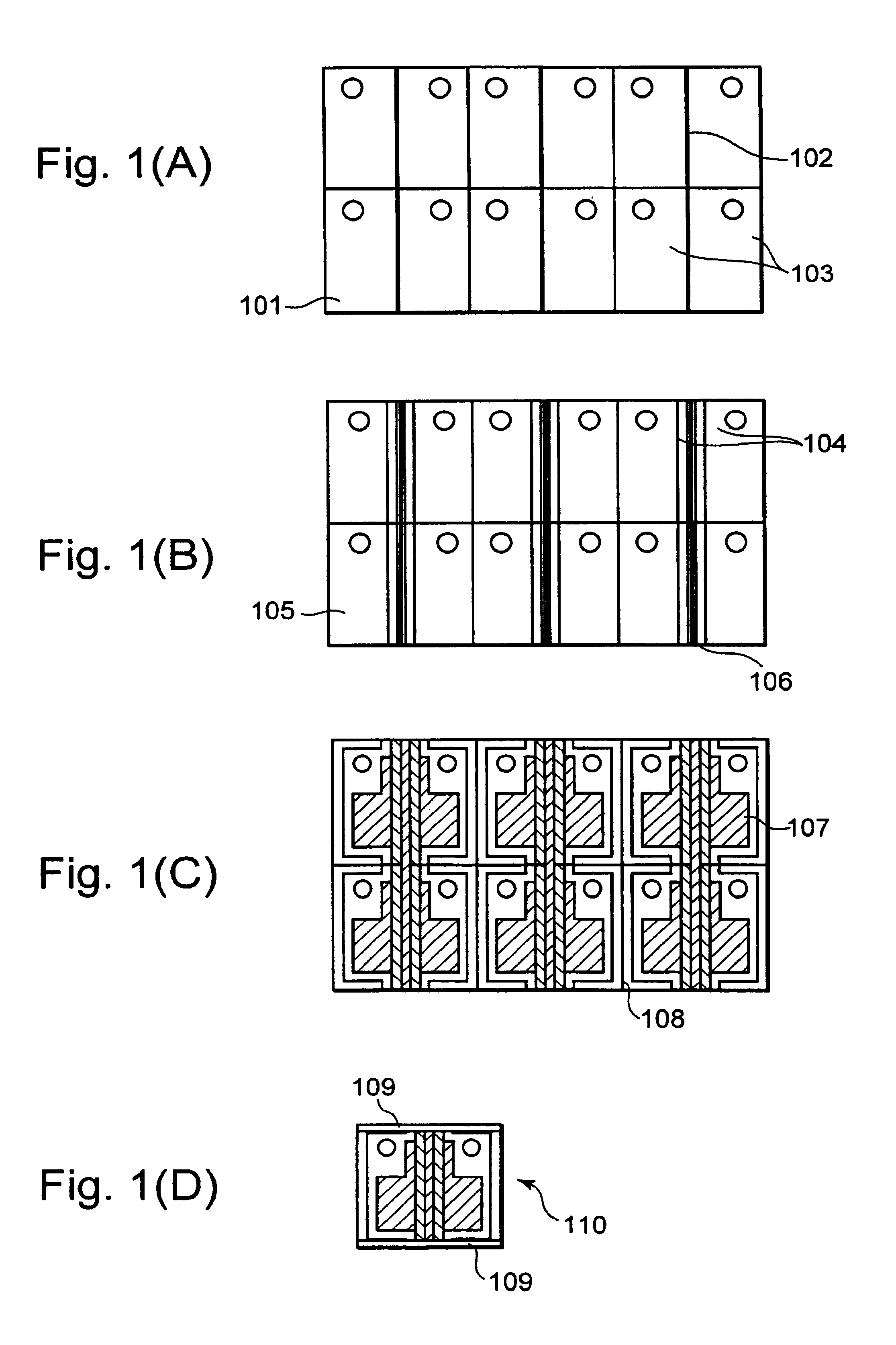
[0014]FIGS. 1(A) through 1(D) are forming process diagrams of a semiconductor chip, showing the present invention.

[0015]As shown in FIG. 1(A), ohmic contact electrode lines 102 and markers 103 are first formed on the junction side of an InP substrate 101 having an active layer and a block layer. The ohmic contact electrode lines 102 and the markers 103 are respectively composed of AuZu and simultaneously formed by lift-off. Thereafter, sintering is performed to ensure ohmic contacts between the ohmic contact electrode lines 102 and the InP substrate 101.

[0016]Next, as shown in FIG. 1(B), the InP substrate 101 is etched to form W channels 104. Thereafter, a silicon oxide film 105 for current narrowing is formed over the whole surface. Further, afterwards, the silicon oxide film 105 is etched to open line patterns 106 of electrode contact portions on their corresponding ohmic contact electrode lines 102.

[0017]As shown in FIG. 1(C), mounting electrodes 107 are respectively formed on th...

second embodiment

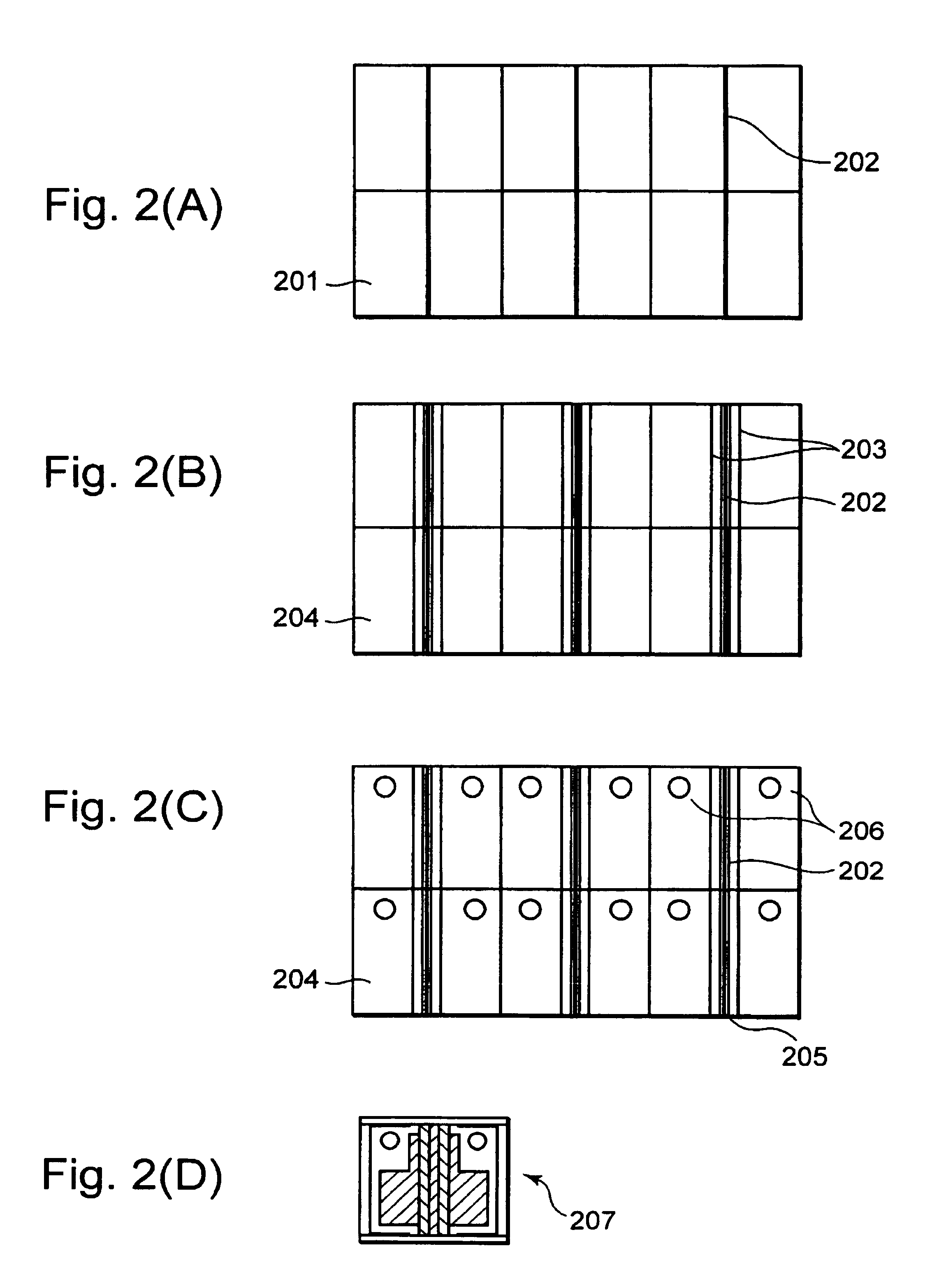
[0021]A second embodiment of the present invention will next be explained with reference to FIGS. 2(A) through 2(D). FIGS. 2(A) through 2(D) are forming process diagrams of a semiconductor chip, showing the present invention.

[0022]As shown in FIG. 2(A), ohmic contact electrode lines 202 are first formed on the junction side of an InP substrate 201 having an active layer and a block layer. The ohmic contact electrode lines 202 are respectively composed of AuZu and formed by lift-off. Thereafter, sintering is performed to ensure ohmic contacts between the ohmic contact electrode lines 202 and the InP substrate 201.

[0023]Next, as shown in FIG. 2(B), the InP substrate 201 is etched to form W channels 203. Thereafter, a silicon oxide film 204 for current narrowing is formed over the whole surface. Further, afterwards, as shown in FIG. 2(C), the silicon oxide film 204 is etched to simultaneously form line patterns 205 of electrode contact portions and markers 206 on their corresponding oh...


PUM


Abstract

A method of manufacturing a semiconductor laser chip has following steps. First, a semiconductor substrate including an active layer and a block layer is provided. An electrode line pattern and a marker are formed on the semiconductor substrate. The semiconductor substrate is etched to form a W channel. Then, an oxide layer is formed on the semiconductor substrate to cover the electrode line pattern and the marker. A part of the oxide layer to form an electrode contact that exposes the electrode line pattern. A mounting electrode is formed on the electrode line pattern. Finally, the semiconductor substrate is divided into a plurality of semiconductor laser chip.

Description

[0001]The rights of priority are claimed under 35 USC §119 of U.S. Provisional Application No. 60 / 413,780, filed Sep. 27, 2002.BACKGROUND OF THE INVENTION[0002]The present invention relates to a method of forming a semiconductor chip, and more specifically to formation of laser chip markers for passive alignment.[0003]The passive alignment has been described in “Synonymous With Alignment-Optical Packaging”, Journal of Japan Institute of Electronics Packaging, Vol. 13, No. 1 (1988), pp 54-56. While a visual type, a mechanical type, and a flip-chip type have been introduced for the passive alignment in the present Journal, the present invention relates to the visual type.[0004]According to the above-described document, the visual type passive alignment is equivalent to one wherein a chip mounter adopted in die bonding of electronic components such as an LSI chip is made high in accuracy. Both a mounting board and an optical chip are provided with eye-alignment markers, and both positi...

Claims


Application Information

Patent Timeline
IPC IPC(8): H01L21/301H01L21/46H01S5/02H01S5/0238H01S5/042H01S5/22
CPCH01S5/0202H01S5/0207H01S5/0425H01S5/2214H01S2301/176H01S5/04254H01S5/02375H01S5/0238
Inventor MURAISHI, MITSUMASA
Owner NEOPHOTONICS SEMICON GK
Why Eureka
Try Eureka