Method of manufacturing an electronic circuit and manufacturing apparatus of an electronic circuit

a manufacturing apparatus and electronic circuit technology, applied in the direction of conductive pattern formation, electrographic process, instruments, etc., can solve the problems of inability to impart an electrostatic property to conductive particles in principle, long time for designing and preparing masks, and large influence on the cost and delivery time of circuit boards

Inactive Publication Date: 2005-12-20
KK TOSHIBA
View PDF6 Cites 10 Cited by
  • Summary
  • Abstract
  • Description
  • Claims
  • Application Information

AI Technical Summary

Problems solved by technology

In both of the methods, however, the need for forming masks used for exposure in advance has caused cost increase and long time for designing and preparing the masks.
In addition, the cost and delivery time of the circuit board have been greatly influenced by the correction of the masks, if the need for the correction should arise.
With such electrophotography, however, it has been impossible in principle to impart an electrostatic property to conductive particles.
It is barely possible to impart the electrostatic property to a metal oxide film, but the formation of a conductive pattern has been difficult due to extreme difficulty in adjusting the thickness and quality of the oxide film and controlling the quantity of electric charges.
Therefore, the use of this pattern as a wiring circuit has not been possible.
Further, in the circuit pattern formed on the ceramic green sheet by the aforementioned method, though the electrical resistance can be lowered to some extent by removing the binder resin by burning, it has been still impossible to obtain sufficient electric conductivity as a wiring circuit.
In addition, the removal of the binder resin by burning is a technique limitedly used for ceramic substrates and cannot be adopted for substrates in which resin such as epoxy resin is used as a base material.
However, conductivity and imparting of the electrostatic property are in a trade-off relation, which has posed such a problem that the increase in metal particle content results in difficulty in controlling the electrostatic property.
Especially, in order to form a microscopic pattern such as a circuit pattern with high precision, controlling the electrostatic property is extremely important, but the industrial production of conductive resin which can achieve both high precision in circuit formation and good electric characteristics has been extremely difficult.
Moreover, this method has not been able to fully satisfy demands such as cost reduction and a shorter cycle of design, production, and so on.

Method used


Image

  • Method of manufacturing an electronic circuit and manufacturing apparatus of an electronic circuit
  • Method of manufacturing an electronic circuit and manufacturing apparatus of an electronic circuit
  • Method of manufacturing an electronic circuit and manufacturing apparatus of an electronic circuit

Examples


first embodiment

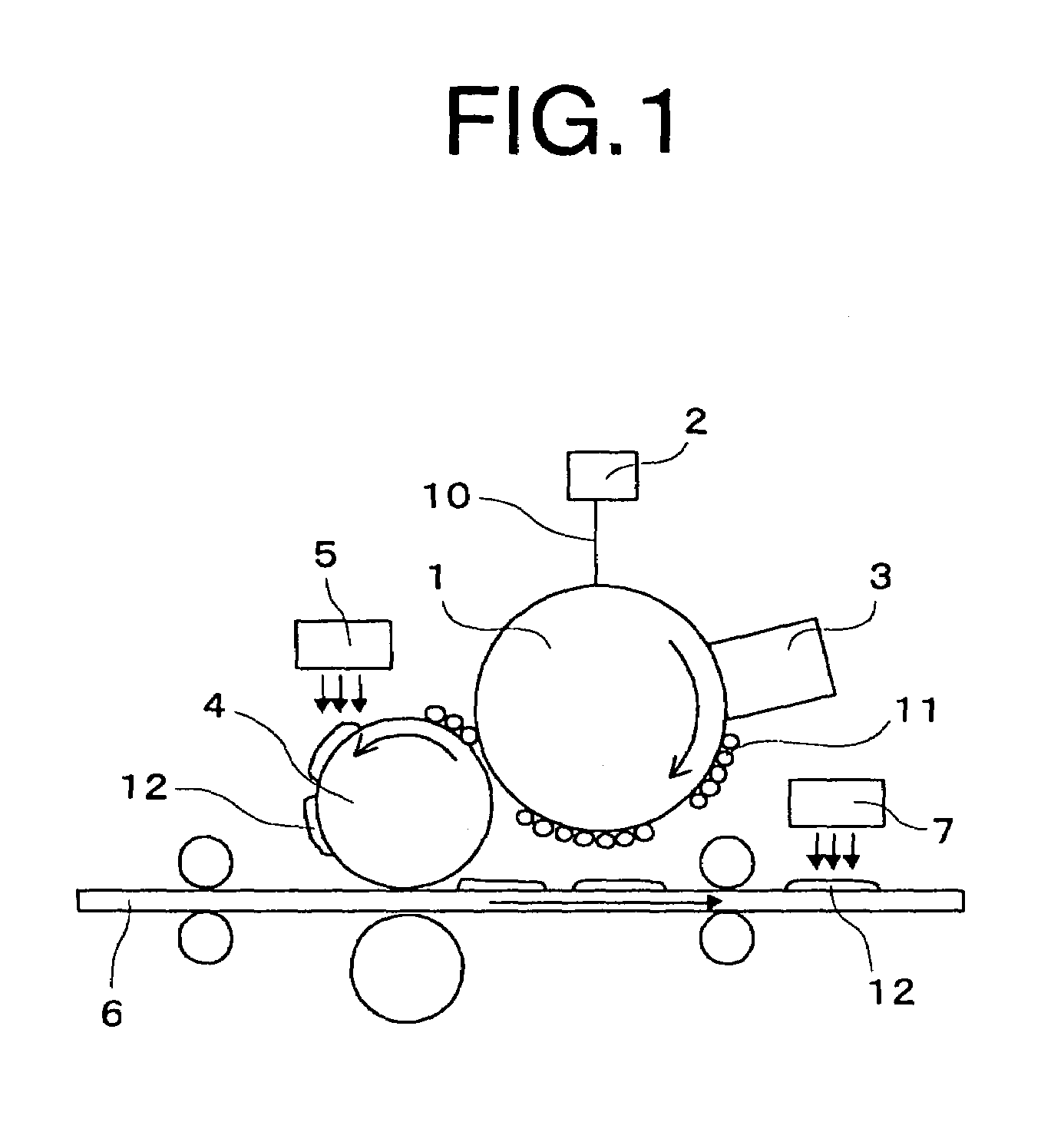
[0038]The first embodiment includes a forming step of an insulating pattern and a forming step of a conductor pattern. The apparatus shown in FIG. 1 is used for forming an insulating pattern. In the forming step of an insulating pattern, the photosensitive drum 1 is first uniformly charged by a not-shown electrifier while being rotated in the arrow direction so that the surface thereof has a certain potential (for example, minus charges). Concrete charging methods includes a scorotron charging method, a roller charging method, a brush charging method, and the like.

[0039]Next, the laser generation / scan unit 2 irradiates the photosensitive drum 1 with a laser beam 10 according to an image signal. Then, the minus charges on a portion irradiated with the laser beam 10 are removed to form an image of charges (electrostatic latent image) in a predetermined pattern on the surface of the photosensitive drum 1.

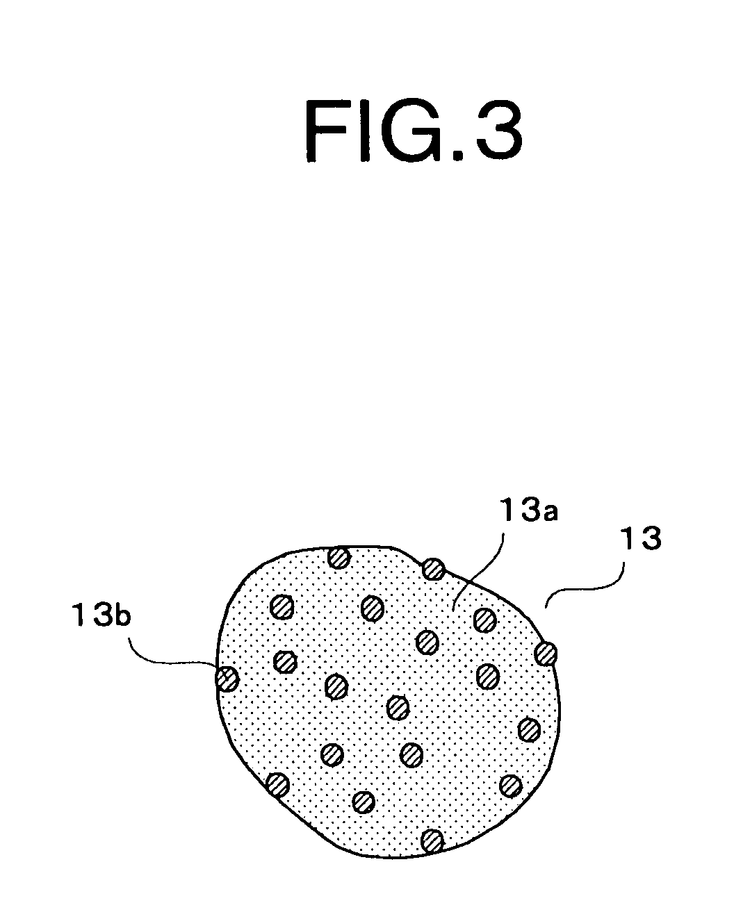
[0040]The developing unit 3 brings electrified resin particles (charged resin part...

second embodiment

[0055]Next, the present invention will be explained.

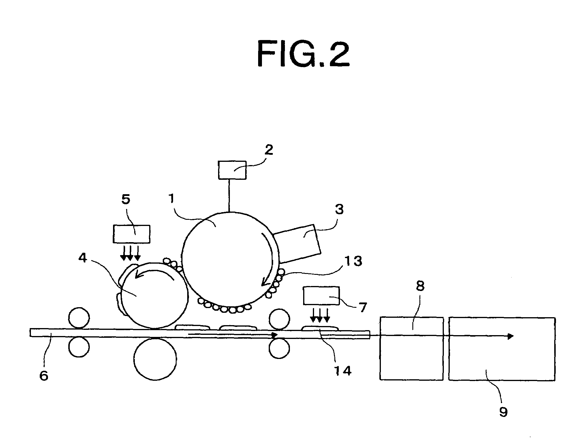
[0056]FIG. 4 is a view schematically showing a forming apparatus of an insulating pattern in the second embodiment of the present invention, and FIG. 5 is a view schematically showing a forming apparatus of a conductor pattern used in the second embodiment. In FIG. 4, the same reference numerals are used to designate the same portions as those in FIG. 1 and the explanation thereof will be omitted. In FIG. 5, the same reference numerals are used to designate the same portions as those in FIG. 2 and the explanation thereof will be omitted. In FIG. 4 and FIG. 5, the reference numeral 15 denotes an electric field generating apparatus.

[0057]The second embodiment includes a forming step of an insulating pattern and a forming step of a conductor pattern. The apparatus shown in FIG. 4 is used for forming an insulating pattern. In the forming step of an insulating pattern, a photosensitive drum 1 is charged while being rotated so that the s...

third embodiment

[0076]Incidentally, it is also possible to etch a copper foil of an ordinary copper clad laminate after a resist pattern is formed on the copper foil in the same manner as in the

[0077]In the fourth embodiment, B-staged thermosetting resin (for example, epoxy resin) containing a fluorescent dye is used. As shown in FIG. 7, similarly to the first embodiment, a pattern of a resin layer 12 is formed on a base material 6, and after the thermosetting resin is heated or irradiated with light to be cured by going through a resin curing unit 7, fluorescence from this resin layer 12 is detected for pattern inspection.

[0078]A pattern inspector is composed of an imaging unit 20 such as a camera that detects the fluorescence, an image processing unit 21, a design data storage memory 22, and a comparison operation unit 23a. The pattern of the resin layer 12 (or a conductive metal-containing resin layer) formed on the base material 6 is formed based on digitalized data inputted in advance. When da...


PUM


Abstract

A method of manufacturing an electronic circuit satisfying demands for cost reduction, diversified small-quantity production, and a shorter cycle of design, manufacture, evaluation, correction, and so on is provided. The method includes at least forming a first pattern or forming a second pattern. Forming the first pattern comprises: forming a visible image on an electrostatic latent image formed on a photosensitive base, by the adhesion of charged particles essentially made of a resin; transferring the visible image onto the intermediate transfer base by the contact and pressurization of the visible image; heating/softening on the intermediate transfer base; and transferring a heated/softened resin layer onto a base material by the contact and pressurization of the resin layer. In forming the second pattern, using charged particles containing conductive metal particulates, a conductor metal layer is formed by electroless plating after a metal-containing resin pattern is transferred similarly to the first pattern formation.

Description

CROSS-REFERENCE TO RELATED APPLICATIONS[0001]This application is based upon and claims the benefit of priorities from the prior Japanese Patent Application No. 2002-205819 filed on Jul. 15, 2002, and the prior Japanese Patent Application No. 2003-272415 filed on Jul. 9, 2003, which claims priority of Japanese Patent Application No. 2002-205819; the entire contents of which are incorporated herein by references.BACKGROUND[0002]1. Field of the Invention[0003]The present invention relates to a method of manufacturing an electronic circuit and a manufacturing apparatus of an electronic circuit.[0004]2. Description of the Related Art[0005]Conventional manufacturing methods of circuit boards are largely classified into the following two methods: (1) a subtractive method and (2) a build-up method.[0006](1) The subtractive method is a method in which a substrate constituted of, for example, a copper (Cu) foil and an insulating layer bonded together is subjected to steps of resist coating, e...

Claims


Application Information

Patent Timeline
Patent Type & Authority Patents(United States)
IPC IPC(8): H01L21/28G03G5/05G03G9/09G03G13/26H01L21/288H01L21/3205H05K3/10H05K3/18H05K3/24H05K3/46
CPCG03G5/056G03G9/0926G03G13/26H05K3/1266H05K3/4664H01L24/19H05K3/246H05K2201/0212H05K2201/0347H05K2203/0425H05K2203/0517H05K2203/0522H05K2203/0537H01L2224/04105H01L2224/32225H01L2224/73267H01L2224/92244H01L2924/15153G03G15/224G03G15/6585G03G15/6591H01L2924/12042H01L2924/15787H01L2924/00
Inventor AOKI, HIDEOTAKUBO, CHIAKIIIDA, ATSUKOHOTTA, YASUYUKIYAMAGUCHI, NAOKO
Owner KK TOSHIBA
Why Eureka
Try Eureka