Nitride-based semiconductor light-emitting device and method of fabricating the same

a technology of nitride-based semiconductors and light-emitting devices, which is applied in the direction of semiconductor lasers, solid-state devices, lasers, etc., can solve the problems of cracks or crystal defects, difficulty in and lattice defects in current blocking layers, so as to achieve the effect of stabilizing transverse light confinemen

Inactive Publication Date: 2005-12-20
EPISTAR CORP
View PDF33 Cites 50 Cited by
  • Summary
  • Abstract
  • Description
  • Claims
  • Application Information

AI Technical Summary

Benefits of technology

[0017]An object of the present invention is to provide a nitride-based semiconductor light-emitting device capable of stabilizing transverse light confinement.
[0018]Another object of the present invention is to provide a nitride-based semiconductor light-emitting device capable of suppressing formation of crystal defects resulting from a contaminant on an interface between a cladding layer and a current blocking layer.
[0019]Still another object of the present invention is to provide a method of fabricating a nitride-based semiconductor light-emitting device capable of easily forming a nitride-based semiconductor light-emitting device capable of stabilizing transverse light confinement.

Problems solved by technology

When the Al composition of the current blocking layers 306 consisting of n-type AlGaN is increased, therefore, strain is applied to the current blocking layers 306 to disadvantageously easily cause cracks or crystal defects such as dislocations in the current blocking layers 306.
Consequently, it is difficult to form the current blocking layers 306 with a large thickness, leading to difficulty in stabilization of transverse light confinement.
When the In composition of the current blocking layers consisting of InGaN is increased, therefore, strain is applied to the current blocking layers to easily cause lattice defects in the current blocking layers.
Also in this case, it is difficult to form the current blocking layers with a large thickness, leading to difficulty in stabilization of transverse light confinement.
Therefore, cracks or lattice defects are easily caused on the current blocking layers 306.
Consequently, it is difficult to thickly form the current blocking layers 306, disadvantageously leading to difficulty in stabilization of transverse light confinement.
Therefore, cracks or lattice defects are easily caused on the current blocking layers.
Also in this case, it is difficult to thickly form the current blocking layers, disadvantageously leading to difficulty in stabilization of transverse light confinement.

Method used


Image

  • Nitride-based semiconductor light-emitting device and method of fabricating the same
  • Nitride-based semiconductor light-emitting device and method of fabricating the same
  • Nitride-based semiconductor light-emitting device and method of fabricating the same

Examples


first embodiment

[0100](First Embodiment)

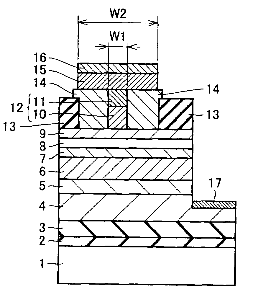
[0101]The structure of a nitride-based semiconductor laser device according to a first embodiment of the present invention is described with reference to FIG. 1. This nitride-based semiconductor laser device according to the first embodiment is a complex refractive index guided laser device.

[0102]In the structure of the nitride-based semiconductor laser device according to the first embodiment, a buffer layer 2 of AlGaN having a thickness of about 15 nm and an undoped GaN layer 3 having a thickness of about 0.5 μm are formed on a sapphire (0001) plane substrate 1 (hereinafter referred to as “sapphire substrate 1”). An n-type contact layer 4, having a mesa portion of about 70 μm in width, consisting of n-type GaN having a thickness of about 4 μm is formed on the undoped GaN layer 3. The sapphire substrate 1 is an example of the “substrate” according to the present invention, and the n-type contact layer 4 is an example of the “nitride-based semiconductor layer...

second embodiment

[0120](Second Embodiment)

[0121]The structure of a nitride-based semiconductor laser device according to a second embodiment of the present invention is described with reference to FIG. 8. The nitride-based semiconductor laser device according to the second embodiment is a real refractive index guided laser device. While the current blocking layer 14 is selectively grown only in the vicinity of the current path portion 12 by using the mask layer 13 in the aforementioned first embodiment, a current blocking layer 33 is selectively grown on step portions 100 thereby forming parts of the current blocking layer 33 having a smaller thickness than that in the vicinity of a current path portion 32 in regions not in the vicinity of the current path portion 32 in the second embodiment. The second embodiment is now described in detail.

[0122]In the structure of the nitride-based semiconductor laser device according to the second embodiment, a buffer layer 22 of AlGaN having a thickness of about...

third embodiment

[0140](Third Embodiment)

[0141]The structure of a nitride-based semiconductor laser device according to a third embodiment of the present invention is described with reference to FIG. 15. The nitride-based semiconductor laser device according to the third embodiment has a real refractive index guided self-aligned structure.

[0142]In the structure of the nitride-based semiconductor laser device according to the third embodiment, a buffer layer 42 of n-type AlGaN having a thickness of about 15 nm, an n-type GaN layer 43 of n-type GaN having a thickness of about 4 μm, an anti-cracking layer 44 of n-type In0.05Ga0.95N having a thickness of about 0.1 μm, an n-type second cladding layer 45 of n-type AlGaN having a thickness of about 1 μm and an n-type first cladding layer 46 of n-type GaN having a thickness of about 50 nm are formed on an n-type Si (111) plane substrate 41 (hereinafter referred to as “n-type Si substrate 41”).

[0143]An MQW emission layer 47 consisting of multiple quantum wel...


PUM


Abstract

A nitride-based semiconductor light-emitting device capable of stabilizing transverse light confinement is obtained. This nitride-based semiconductor light-emitting device comprises an emission layer, a cladding layer, formed on the emission layer, including a first nitride-based semiconductor layer and having a current path portion and a current blocking layer, formed to cover the side surfaces of the current path portion, including a second nitride-based semiconductor layer, while the current blocking layer is formed in the vicinity of the current path portion and a region having no current blocking layer is included in a region not in the vicinity of the current path portion. Thus, the width of the current blocking layer is reduced, whereby strain applied to the current blocking layer is relaxed. Consequently, the thickness of the current blocking layer can be increased, thereby stabilizing transverse light confinement.

Description

BACKGROUND OF THE INVENTION[0001]1. Field of the Invention[0002]The present invention relates to a nitride-based semiconductor light-emitting device and a method of fabricating the same, and more particularly, it relates to a nitride-based semiconductor light-emitting device comprising a current blocking layer and a method of fabricating the same.[0003]2. Description of the Background Art[0004]A nitride-based semiconductor laser device, which is one of nitride-based semiconductor light-emitting devices, is expected as an advanced light source for a large capacity disk, and subjected to active development. A well-known general nitride-based semiconductor laser device has current blocking layers consisting of a material having reverse conductivity to a nitride-based semiconductor layer forming a ridge portion on side portions of the ridge portion serving as a current path portion. This nitride-based semiconductor laser device is disclosed in Japanese Patent Laying-Open No. 10-321962 (...

Claims


Application Information

Patent Timeline
Patent Type & Authority Patents(United States)
IPC IPC(8): H01L33/14H01L33/32H01S5/22H01S5/223H01S5/323
CPCB82Y20/00H01L33/145H01S5/2231H01S5/32341H01S5/34333H01L33/32H01S5/0213H01S5/0422H01S5/0425H01S5/2022H01S5/204H01S5/2205H01S5/2206H01S5/2216H01S5/2219H01S5/2224H01S5/2226H01S5/3063H01S5/3213H01S2301/173H01S2301/18H01S2304/04H01S2301/176H01S5/04254H01S5/04257
Inventor HATA, MASAYUKINOMURA, YASUHIKOINOUE, DAIJIRO
Owner EPISTAR CORP
Why Eureka
Try Eureka