Reduced surface field technique for semiconductor devices

a semiconductor device and surface field technology, applied in semiconductor devices, semiconductor/solid-state device details, electrical equipment, etc., can solve the problems of excessive complexity of the process for manufacturing power devices, the inability to achieve desirable characteristics of other types of devices such as bipolar transistors and cmos, and the failure of the ldmos devi

Inactive Publication Date: 2005-12-27
SEMICON COMPONENTS IND LLC
View PDF13 Cites 45 Cited by
  • Summary
  • Abstract
  • Description
  • Claims
  • Application Information

AI Technical Summary

Problems solved by technology

When the extension of the depletion region passes a limit, a breakdown will occur in the LDMOS device.
Whenever it is desired to manufacture a single device comprising transistors of various types of devices (e.g., bipolar transistor, CMOS (complementary MOS), and DMOS (double-diffused MOS)), such as a BCD (bipolar-CMOS-DMOS) device, a conflict may arise.
For if the thickness of the epitaxial layer is increased to achieve a higher breakdown voltage for the DMOS it then becomes increasingly difficult to achieve desirable characteristics in the device of other types such as bipolar transistor and CMOS.
Alternatively, if the various desirable thickness of epitaxial layers desirable for each type of device are implemented, then the process for manufacturing power devices becomes excessively complex due to an excessive number of steps required in the process of forming the device.
Furthermore, increasing manufacturing process complexity drives up costs.

Method used


Image

  • Reduced surface field technique for semiconductor devices
  • Reduced surface field technique for semiconductor devices
  • Reduced surface field technique for semiconductor devices

Examples


Embodiment Construction

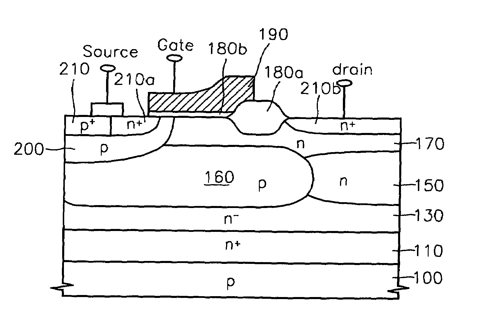
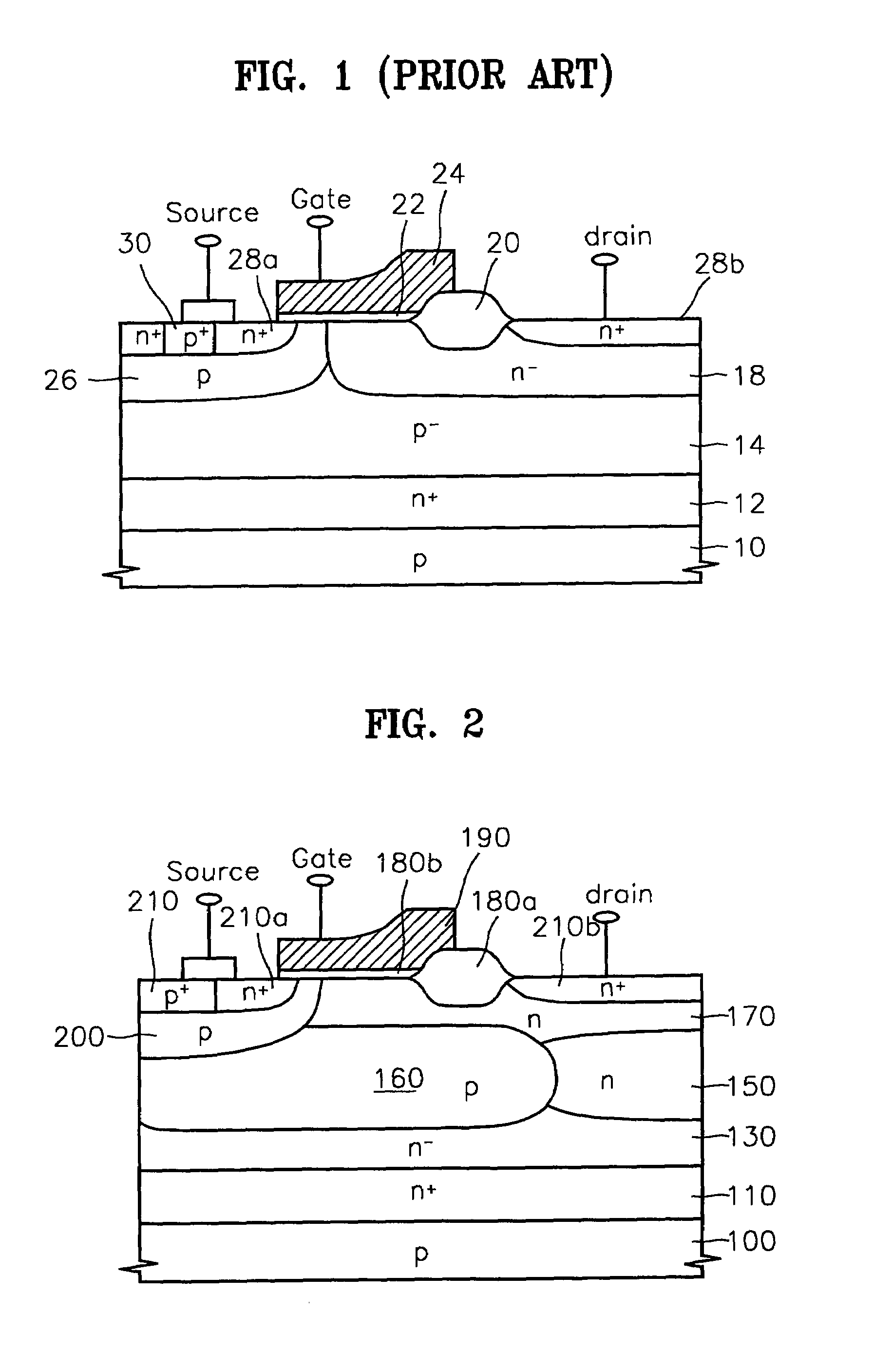
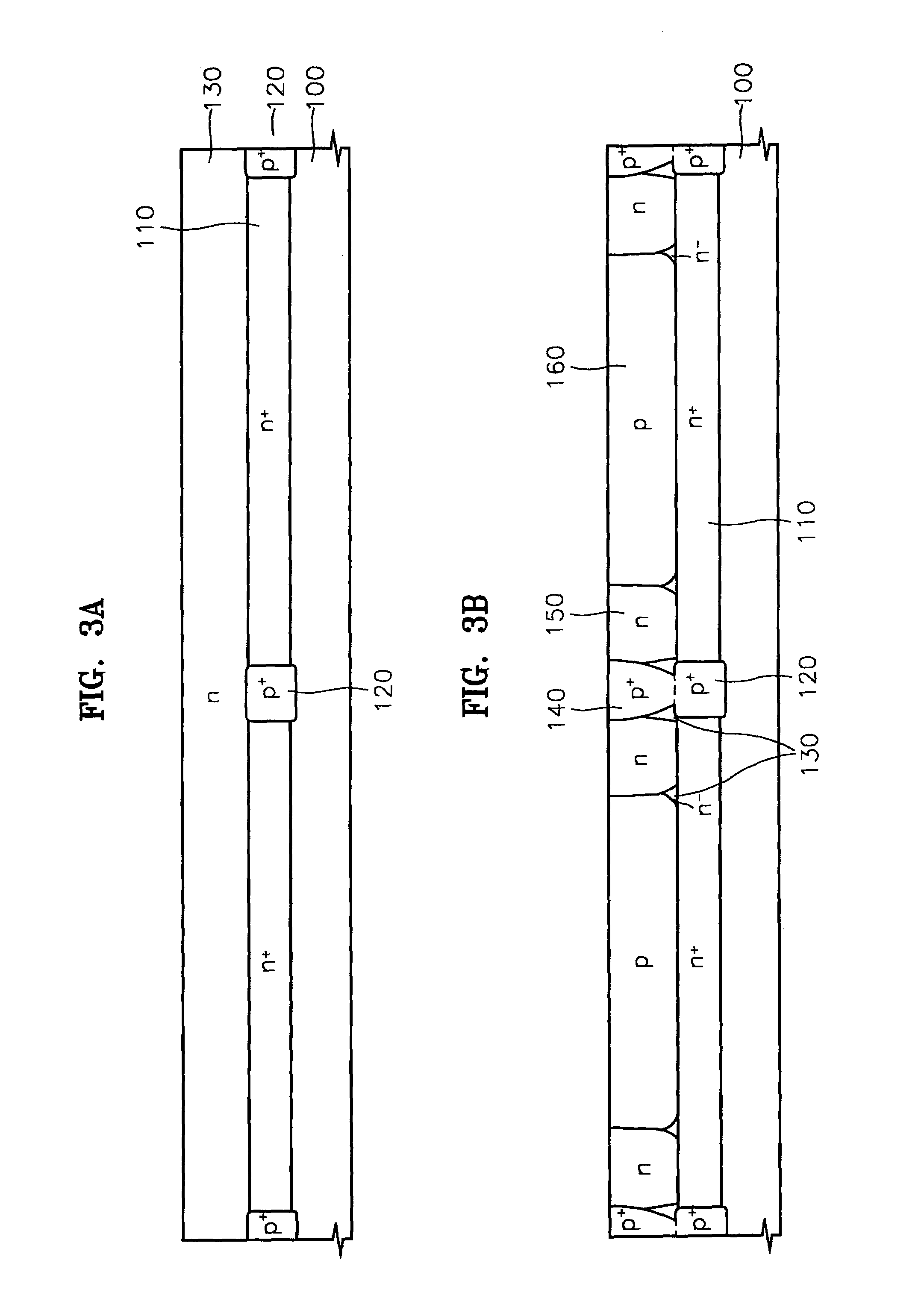
[0019]Accordingly, it is necessary to develop a power device having a breakdown voltage not related to the thickness of an epitaxial layer.

[0020]The present invention is described below with reference to the accompanying drawings, in which a preferred embodiment of the invention is shown. This invention may, however, be embodied in many different forms, and should not be construed as being limited to the embodiment set forth herein; rather, this embodiment is provided so that this disclosure will be thorough and complete and will fully convey the concept of the present invention to those skilled in the art. In the drawings, the thickness of layers and regions may be exaggerated for clarity. Like reference numerals in different drawings refer to like and corresponding parts and their description may be omitted. It will also be understood that when a layer is referred to as being “on” another layer or a substrate, it can be directly on the other layer or the substrate, or intervening ...


PUM


Abstract

A power device and a method for manufacturing the same are provided. The power device comprises a first conductive semiconductor substrate; a second conductive buried layer formed to a certain depth within the semiconductor substrate; a second conductive epitaxial layer formed on the conductive buried layer; a first conductive well formed within the conductive epitaxial layer; a second conductive well formed within the second conductive epitaxial layer, on both sides of the first conductive well; a second conductive drift region formed in predetermined portions on the first and the second conductive well; and a lateral double diffused MOS transistor formed in the second conductive drift region. The breakdown voltage of the power device is controlled according to a distance between the first conductive well and the second conductive buried layer.

Description

RELATED APPLICATION[0001]This application claims priority to Korean Patent Application No. 2002-25623, entitled, “POWER DEVICE AND METHOD FOR MANUFACTURING THE SAME” filed on May 9, 2002.FIELD OF THE INVENTION[0002]The present invention relates generally to MOS (metal-oxide semiconductor) ICs (integrated circuits), and more particularly, to ICs comprising a LDMOS (lateral double-diffused MOS) device capable of having a high breakdown voltage and a method for manufacturing such a device.BACKGROUND OF THE INVENTION[0003]For some applications of semiconductor IC devices, it is desirable for the IC devices to operate at relatively high voltages, for example, in a range of 15–80 volts. LDMOS devices have been widely used as devices for control, logic and especially power switching. LDMOS devices may have a relatively high breakdown voltage so as to insulate high voltages. In addition, LDMOS devices may preferably have a low “ON” state resistance so as to provide good switching characteri...

Claims


Application Information

Patent Timeline
IPC IPC(8): H01L21/336H01L23/58H01L27/088H01L29/06H01L29/08H01L29/10H01L29/78
CPCH01L27/088H01L29/1095H01L29/66681H01L29/7816H01L29/0634H01L29/0847H01L29/0878H01L29/42368H01L29/78
Inventor KWON, TAE-HUNKIM, CHOEL-JOONGLEE, SUK-KYUN
Owner SEMICON COMPONENTS IND LLC
Why Eureka
Try Eureka