
Liquid crystal display having reduced flicker

Inactive Publication Date: 2006-01-03
INNOLUX CORP
View PDF23 Cites 20 Cited by
  • Summary
  • Abstract
  • Description
  • Claims
  • Application Information

AI Technical Summary

Benefits of technology

[0012]It is therefore a objective of the claimed invention to provide a liquid crystal display (LCD) having reduced flicker to solve the above-mentioned problem.
[0013]According to the claimed invention, a liquid crystal display (LCD) having reduced flicker includes a plurality of signal lines, a plurality of scanning lines, and a plurality of pixels. Each pixel includes a liquid crystal cell having a pixel electrode, a storage capacitor, and a switching transistor. The switching transistor includes a gate electrode connected to one of the scanning lines, a drain electrode connected to one of the signal lines, and a source electrode connected to the pixel electrode. An overlapping region is between the gate electrode and the source electrode. The area of the overlapping region increases by increasing the distance between an input end of the scanning line corresponding to the overlapping region and the pixel electrode corresponding to the overlapping region.
[0014]It is an advantage that the claimed invention adjusts the capacitance between the gate electrode and the source electrode of the thin film transistor by varying the areas of the overlapping regions so that feed-through voltages of all pixels are approximately equal. There are no changes occurring to the storage capacitors and the width of the scanning lines. Thus, the storage capacitors can help the liquid crystal cells hold the electric charges effectively. The aperture ratio of the LCD apparatus can be improved as well.

Problems solved by technology

Accordingly, it is difficult to compensate feed-through voltages for all pixels by adjusting the voltage of the common counter electrode.
Therefore, it is hard to provide a TFT-LCD without flicker.
As a result, it is hard for such storage capacitor with low capacitance to help the liquid crystal cells hold electric charges.

Method used


Image

  • Liquid crystal display having reduced flicker
  • Liquid crystal display having reduced flicker
  • Liquid crystal display having reduced flicker

Examples


Embodiment Construction

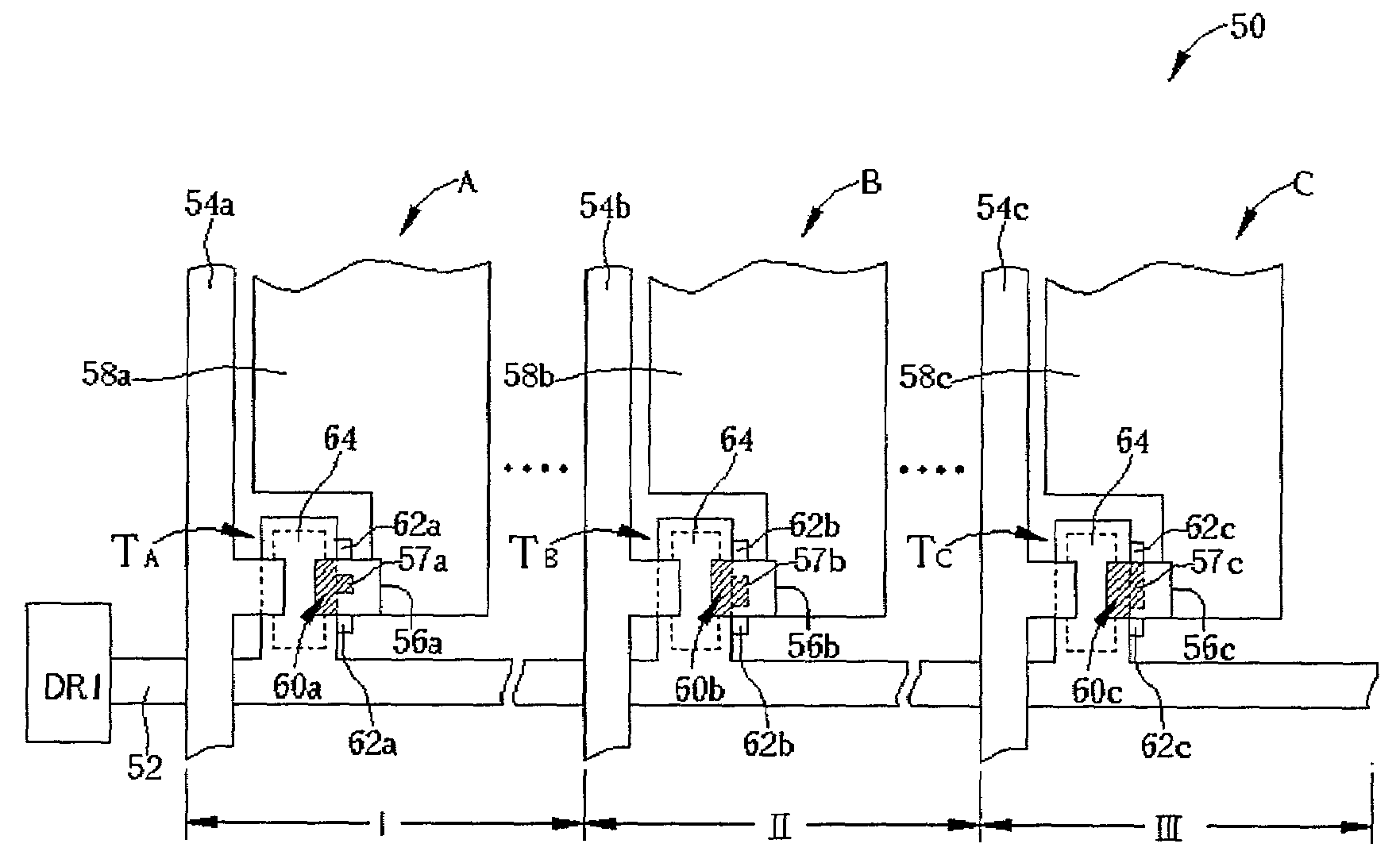
[0021]Referring to FIG. 4, FIG. 4 is a top view of a pixel array of a TFT-LCD according to the present invention. As shown in FIG. 4, a pixel array 50 comprises a scanning line 52 electrically connected to a scanning line control circuit (DR1), signal lines 54a, 54b, 54c, and pixels A, B, C, which respectively correspond to pixels A, B, C shown in FIG. 1. Pixels A, B, C comprise thin film transistors TA, TB, TC respectively, and their corresponding liquid crystal cells. The gate electrodes of thin film transistors TA, TB, TC are connected to the scanning line 52. The drain electrodes of thin film transistors TA, TB, TC are connected to signal lines 54a, 54b, 54c respectively. The source electrodes of thin film transistors TA, TB, TC are respectively connected to pixel electrodes 58a, 58b, 58c of the liquid crystal cells. Region 60a (drawn as slash) is an overlapping region of the scanning line 52 and the source electrode 56a. Region 60b (drawn as slash) is an overlapping region of t...


PUM


Abstract

A liquid crystal display (LCD) having reduced flicker includes a plurality of signal lines, a plurality of scanning lines, and a plurality of pixels. Each pixel includes a liquid crystal cell having a pixel electrode, a storage capacitor, and a switching transistor. The switching transistor includes a gate electrode connected to one of the scanning lines, a drain electrode connected to one of the signal lines, and a source electrode connected to the pixel electrode. An overlapping region is between the gate electrode and the source electrode. The area of the overlapping region increases by increasing the distance between an input end of the scanning line corresponding to the overlapping region and the pixel electrode corresponding to the overlapping region.

Description

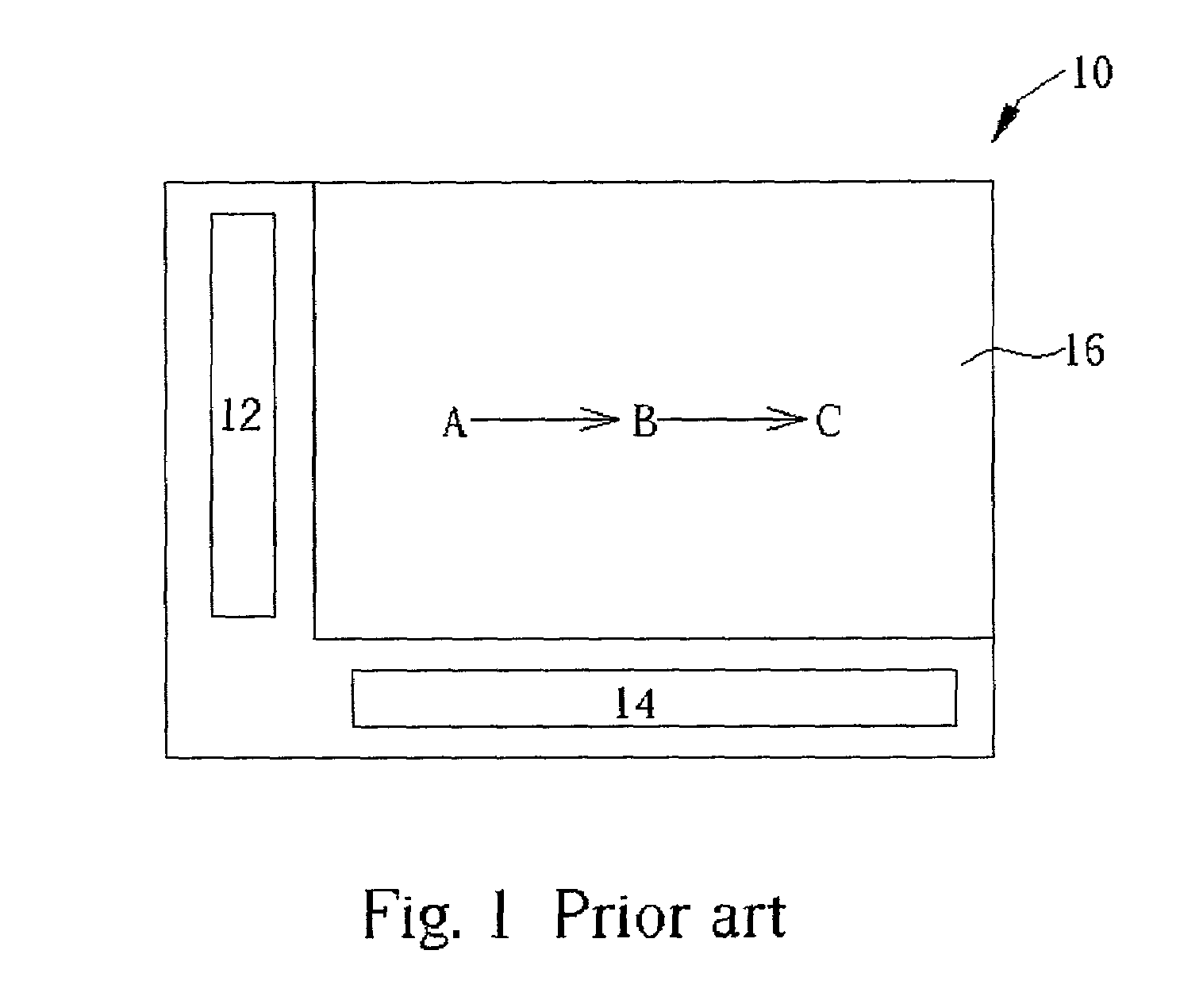
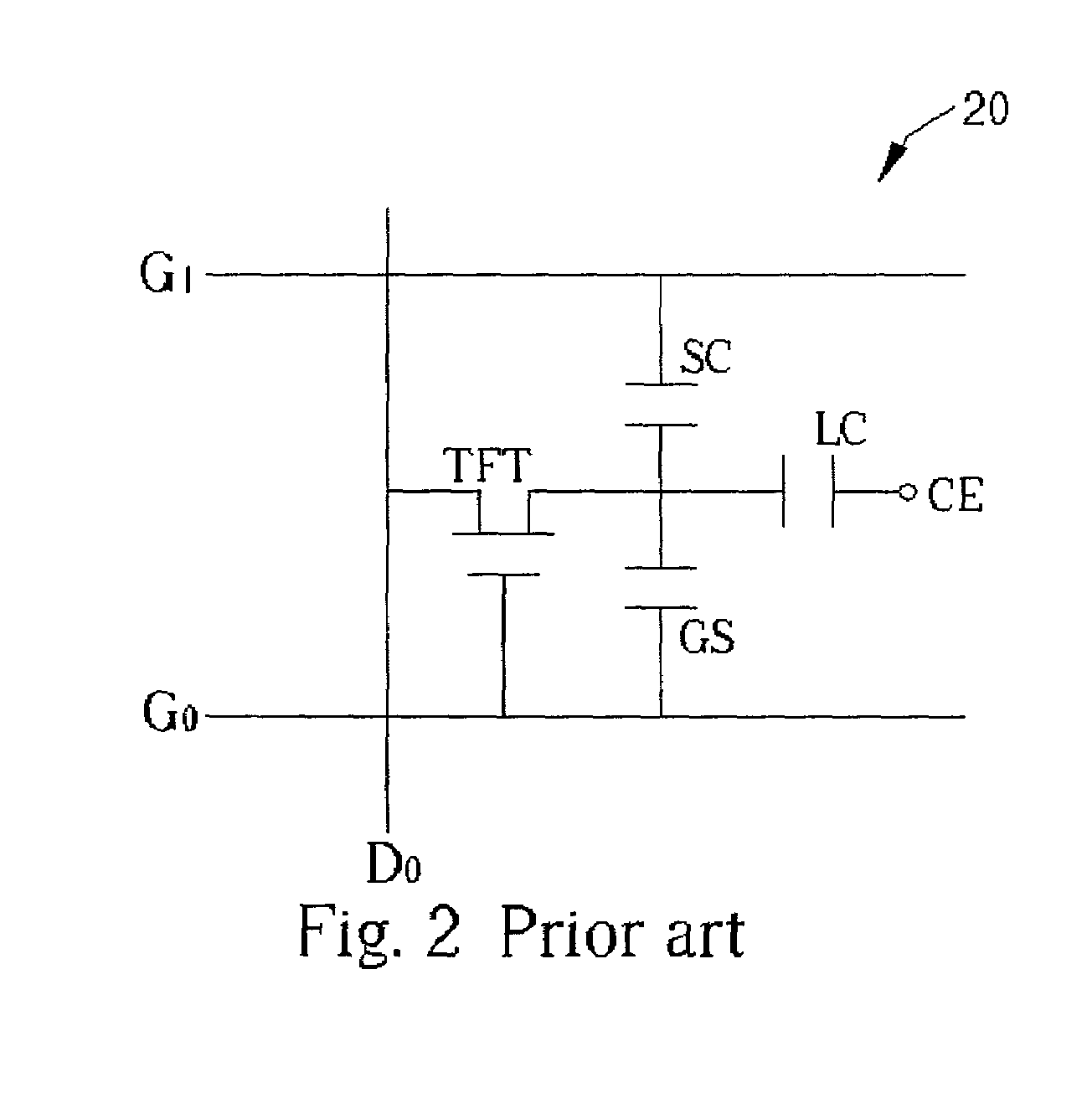
BACKGROUND OF INVENTION[0001]1. Field of the Invention[0002]The present invention relates to a liquid crystal display, and more particularly, to a liquid crystal display having reduced flicker.[0003]2. Description of the Prior Art[0004]A thin film transistor display, such as a thin film transistor liquid crystal display (TFT-LCD), utilizes many thin film transistors, in conjunction with other elements such as capacitors and bonding pads, arranged in a matrix as switches for driving liquid crystal molecules to produce brilliant images. The advantages of the TFT-LCD over a conventional CRT monitor include better portability, lower power consumption, and lower radiation. Therefore, the TFT-LCD is widely used in various portable products, such as notebooks, personal data assistants (PDA), electronic toys, etc.[0005]Referring to FIG. 1 and FIG. 2. FIG. 1 is a schematic diagram of a prior art TFT-LCD 10. FIG. 2 is an equivalent circuit diagram of the TFT-LCD 10. The TFT-LCD 10 comprises a...

Claims


Application Information

Patent Timeline
IPC IPC(8): G02F1/1343G02F1/1345G02F1/1368G02F1/136H01L21/336H01L29/786
CPCG02F1/136213H01L29/42384H01L29/41733G02F1/1368G02F1/136286
Inventor LEE, HSIN-TAWU, CHAO-WEN
Owner INNOLUX CORP
Learn More