Magnetoresistance effect device and magnetoresistance effect head comprising the same, and magnetic recording/reproducing apparatus

Inactive Publication Date: 2006-01-03
PANASONIC CORP
View PDF15 Cites 4 Cited by
  • Summary
  • Abstract
  • Description
  • Claims
  • Application Information

AI Technical Summary

Benefits of technology

[0009]That is, a magnetoresistive element according to the present invention includes a first magnetic layer (free layer), a nonmagnetic layer, a second magnetic layer (pinned layer) laminated to the first magnetic layer through the nonmagnetic layer, and a magnetization rotation suppressing layer for suppressing magnetization rotation of the second magnetic layer. In the magnetoresistive element, the magnetization of the first magnetic layer is rotated more easily by an external magnetic field than

Problems solved by technology

Since the use of FeMn as a material for the magnetization rotation suppressing layer results in a small MR ratio, and the corrosion resistance provided by FeMn itself is not sufficiently high, PtMn- and NiMn-based materials have been used for reproduction magnetic heads for hard disks.
Considering that further increases in magnetic recording

Method used


Image

  • Magnetoresistance effect device and magnetoresistance effect head comprising the same, and magnetic recording/reproducing apparatus
  • Magnetoresistance effect device and magnetoresistance effect head comprising the same, and magnetic recording/reproducing apparatus
  • Magnetoresistance effect device and magnetoresistance effect head comprising the same, and magnetic recording/reproducing apparatus

Examples


Example

(Example 1)

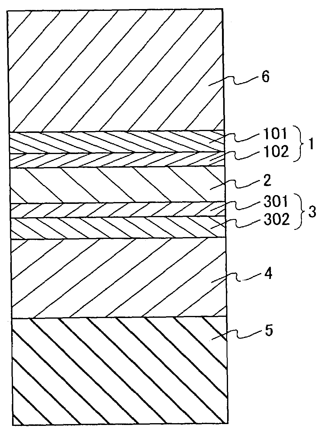
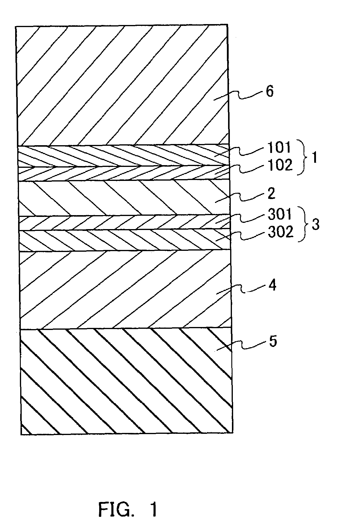
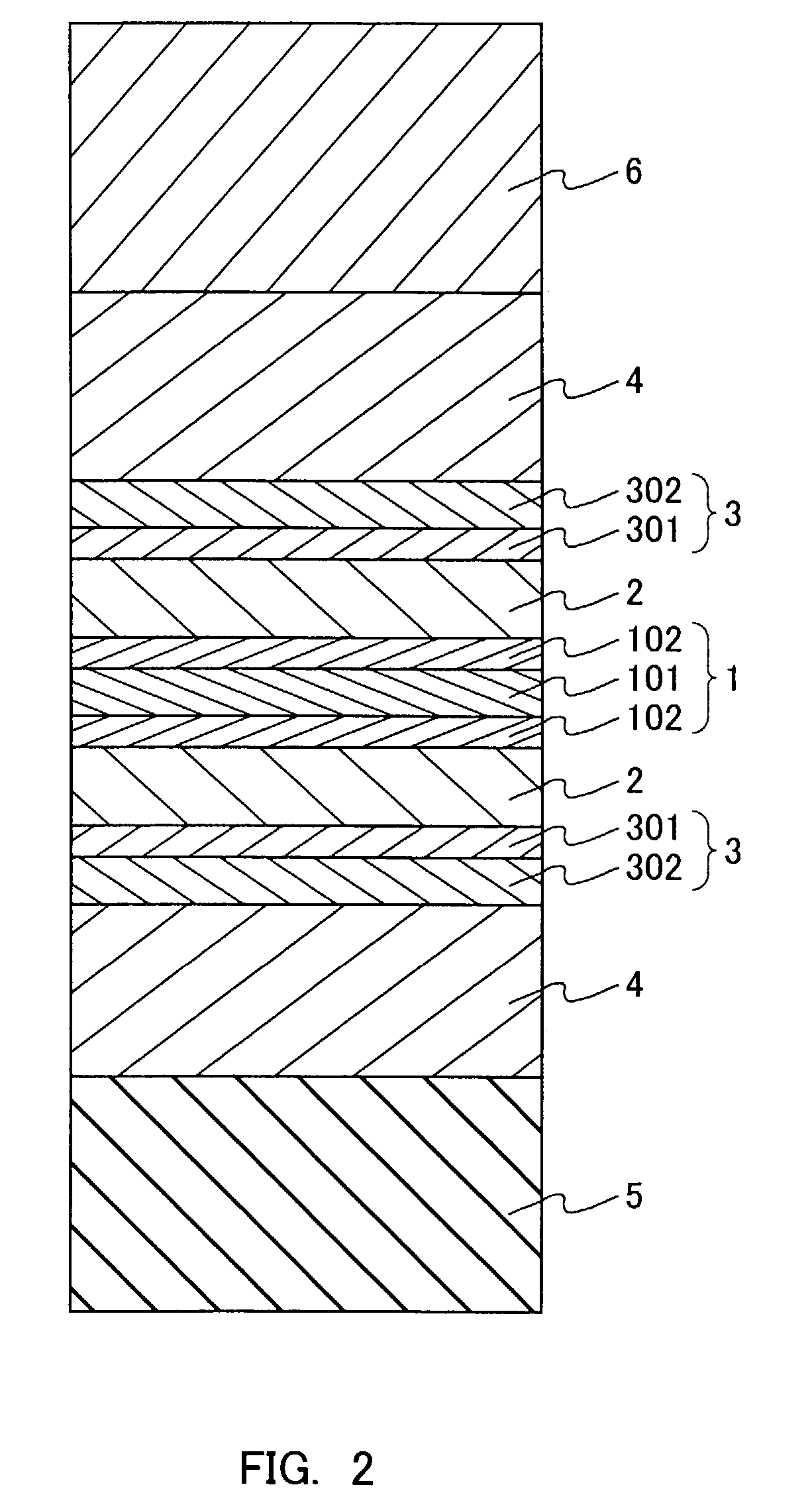
[0051]A magnetoresistive element having a configuration shown in FIG. 8 was fabricated by using a multi-sputtering device. As a material for a substrate 7, Si was used. A Cu film, a Pt—Mn film and a Co—Fe film were formed as a lower electrode 5 (used also as a base layer), a magnetization rotation suppressing layer 4, and a pinned magnetic layer 302, respectively. Further, Fe films were formed as interface magnetic layers 301 and 102. Furthermore, a Cr film, a Ni—Fe film and a Cu film were formed as a nonmagnetic layer 2, a soft magnetic layer 101 and an upper electrode 6, respectively. By using a vacuum chamber exhausted to a pressure of not more than 1×10⁻⁸ Torr, sputtering was performed while feeding an Ar gas so that a pressure of about 0.8 m Torr was attained.

[0052]The film configuration of the element thus fabricated is shown below along with the thicknesses of the respective films (hereinafter, film thicknesses are expressed in nm).[0053]Element A: Substrate / Cu (50...

Example

(Example 2)

[0064]In the same manner as in Example 1, an MR element having a structure shown in FIG. 9 was fabricated. However, in this case, although shown to be a single layer, a pinned layer 3 was formed of a synthetic ferrimagnetic pinned layer of CoFe / Ru / CoFe. A glass substrate was used as a substrate 7, and Cu films were used as a lower electrode 5 and an upper electrode 6. Further, a Ni—Mn alloy film, a Ru film, a Co0.9Fe0.1 alloy film were used as a magnetization rotation suppressing layer 4, a nonmagnetic layer 2, and a free layer 1, respectively. No interface magnetic layer was formed in this case. The film configuration of this element is shown below.[0065]Element C: Substrate / Cu (500) / Ta (3) / Ni0.5Mn0.5 (30) / Co0.9Fe0.1 (2) / Ru (0.7) / Co0.9Fe0.1 (3) / Ru (2.5) / Co0.9Fe0.1 (2) / Ru (2.5) / Co0.9Fe0.1 (3) / Ru (0.7) / Co0.9Fe0.1 (2) / Ni0.5Mn0.5 (30) / Cu

[0066]In this configuration, a Ta film functions as a base film for improving a property of the magnetization rotation suppressing layer. In...


PUM


Abstract

In the present invention, a thin film whose main component is a metal having a specific resistance of 4 μΩ·cm to 200 μΩ·cm is used as a nonmagnetic layer of a so-called CPP-GMR element. Therefore, even when an area of the element becomes limited, the element is not increased excessively in resistance. Thus, even when a magnetic gap is narrow, a large output can be obtained.

Description

[0001]This application is a 371 of PCT / JP01 / 05334 filed Jun. 21, 2001.TECHNICAL FIELD[0002]The present invention relates to a magnetoresistive element, a magnetoresistive head and a magnetic recording and reproducing device such as a hard disk device using the magnetoresistive element.BACKGROUND ART[0003]In recent years, hard disk drives have had considerably increased magnetic recording density. In such a trend, significant advances also have been made in reproduction magnetic head technology. Particularly, the use of a spin valve type magnetoresistive element (MR element) utilizing a giant magnetoresistive effect (GMR) allows the sensitivity of a magnetoresistive head (MR head) to be improved substantially.[0004]The spin valve type MR element includes two ferromagnetic layers and a nonmagnetic layer interposed between the two magnetic layers. The magnetization direction of one of the ferromagnetic layers (pinned layer) is fixed by an exchange bias magnetic field generated from a m...

Claims


Application Information

Patent Timeline
IPC IPC(8): G11B5/39G01R33/09H01F10/32H01L43/08
CPCB82Y10/00B82Y25/00G01R33/093G11B5/3903H01L43/08H01F10/324H01F10/3268H01F10/3272G11B5/3909G11B2005/3996H10N50/10G11B5/39
Inventor KAWAWAKE, YASUHIROSUGITA, YASUNARISAKAKIMA, HIROSHI
Owner PANASONIC CORP
Why Eureka
Try Eureka