Semiconductor memory device

Inactive Publication Date: 2006-01-03
PANASONIC CORP
View PDF5 Cites 26 Cited by
  • Summary
  • Abstract
  • Description
  • Claims
  • Application Information

AI Technical Summary

Benefits of technology

[0017]Therefore, with the foregoing in mind, it is an object of the present invention to provide a semiconductor memory device capable of supplying an o

Problems solved by technology

First, as the number of options regarding a start timing of the sense amplifier circuit 903 is increased, more replica cells 909 need to be provided. Furtherm

Method used


Image

  • Semiconductor memory device
  • Semiconductor memory device
  • Semiconductor memory device

Examples


embodiment 1

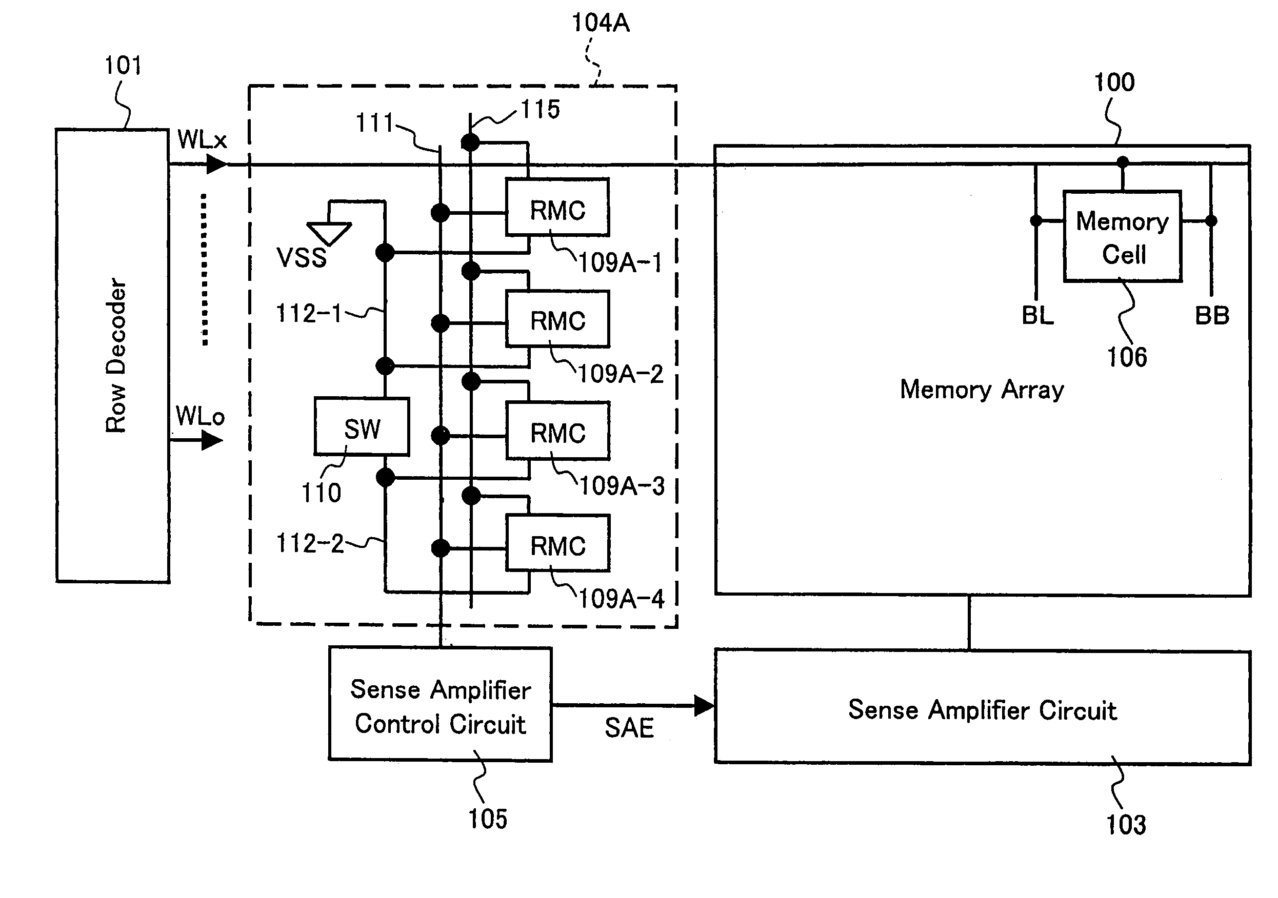
[0047]FIG. 1 is a functional block diagram showing an exemplary configuration of a semiconductor memory device according to Embodiment 1 of the present invention. In FIG. 1, the semiconductor memory device of the present embodiment includes a memory array 100 including a plurality of memory cells 106, a row decoder 101 connected to the memory array 100, a sense amplifier circuit 103 for amplifying data read from selected memory cells 106 to bit lines BL, BB, a replica circuit 104A, and a sense amplifier control circuit 105 for supplying a sense amplifier starting signal SAE to the sense amplifier circuit 103.

[0048]The replica circuit 104A includes a plurality of replica cells 109A-1, 109A-2, 109A-3, and 109A-4 (hereinafter, which may be referred to collectively as 109A) having the same elements as those of the memory cells 106, driven via a dummy bit line 115, and outputting signals with levels corresponding to the stage number to a common replica bit line (RBL) 111, and a switching...

embodiment 2

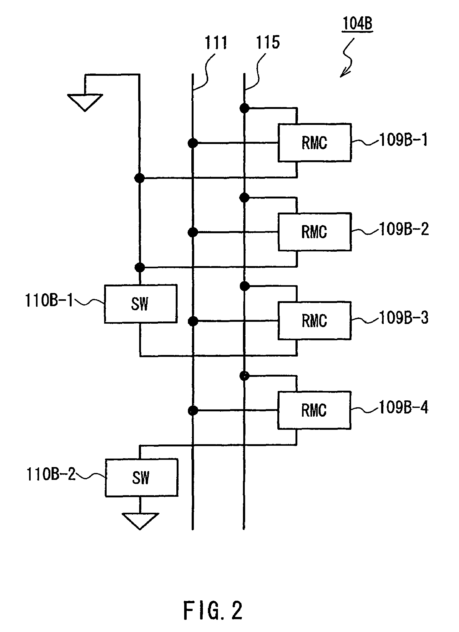
[0054]FIG. 2 is a functional block diagram showing an exemplary configuration of a replica circuit in a semiconductor memory device according to Embodiment 2 of the present invention. In FIG. 2, the replica circuit 104B in the present embodiment includes replica cells 109B-1, 109B-2, 109B-3, and 109B-4 (hereinafter, which may be referred to collectively as 109B), and switching circuits 110B-1 and 110B-2 (hereinafter, which may be referred to collectively as 110B).

[0055]When the replica cells are selected in the same way as in Embodiment 1, a current may be limited by passing through the switching circuits, resulting in less current than originally expected. In order to avoid this, the switching circuits 110B-1 and 110B-2 are provided respectively on different power lines. Because of this, a current will not be limited by passing through the switching circuits 110B.

[0056]As described above, according to the present embodiment, by providing the switching circuits 110B on a plurality o...

embodiment 3

[0057]FIG. 3 is a functional block diagram showing an exemplary configuration of a replica circuit in a semiconductor memory device according to Embodiment 3 of the present invention. In FIG. 3, a replica circuit 104C in the present embodiment includes replica cells 109C-1, 109C-2, 109C-3, and 109C-4 (hereinafter, which may be referred to collectively as 109C), and switching circuits 110C-1 and 110C-2 (hereinafter, which may be referred to collectively as 110C).

[0058]In order to optimize the start timing of a sense amplifier by pulling out the replica bit line 111 to an intended potential, fine adjustment is required. Furthermore, when replica cells are selected in the same way as in Embodiment 1, a current may be limited by passing through the switching circuits, resulting in less current than originally expected. In order to avoid this, by providing a plurality of switching circuits 110C-1 and 110C-2 on one power line, the current amount to be pulled out from a bit line is limited...


PUM


Abstract

A semiconductor memory device includes a replica circuit including a plurality of replica cells (RMC) having the same elements as those of memory cells in a memory array and outputting signals with levels in the stage number to a common replica bit line, and a sense amplifier control circuit for receiving a signal of the replica bit line to control a timing of a signal SAE for starting a sense amplifier circuit. The replica circuit includes a switching circuit (SW) for switching the stage number of the replica cells to be activated among the plurality of replica cells in a programmable manner.

Description

BACKGROUND OF THE INVENTION[0001]1. Field of the Invention[0002]The present invention relates to a semiconductor memory device generating a start timing signal of a sense amplifier circuit, using a replica circuit including replica cells having the same configuration as that of memory cells included in a memory array.[0003]2. Description of the Related Art[0004]There are a number of methods for generating a timing signal of a sense amplifier for amplifying data read from memory cells and allowing a read timing of the memory cells to follow the variation due to a process, a voltage, or the like in a conventional semiconductor memory device. Among them, there is a method for varying a timing signal in a programmable manner, using a replica circuit. Hereinafter, this method will be described.[0005]FIG. 11 is a functional block diagram (see U.S. Pat. No. 6,172,925) showing an exemplary configuration of a conventional semiconductor memory device. In FIG. 11, the conventional semiconducto...

Claims


Application Information

Patent Timeline
IPC IPC(8): G11C7/02G11C11/419G11C7/10G11C7/22G11C11/413H01L21/8244H01L27/11
CPCG11C7/1045G11C7/227G11C7/22G11C2207/2281G11C5/063G11C7/08G11C11/412G11C11/417
Inventor OHTSUKI, HIROHISASUZUKI, TOSHIKAZU
Owner PANASONIC CORP
Why Eureka
Try Eureka