

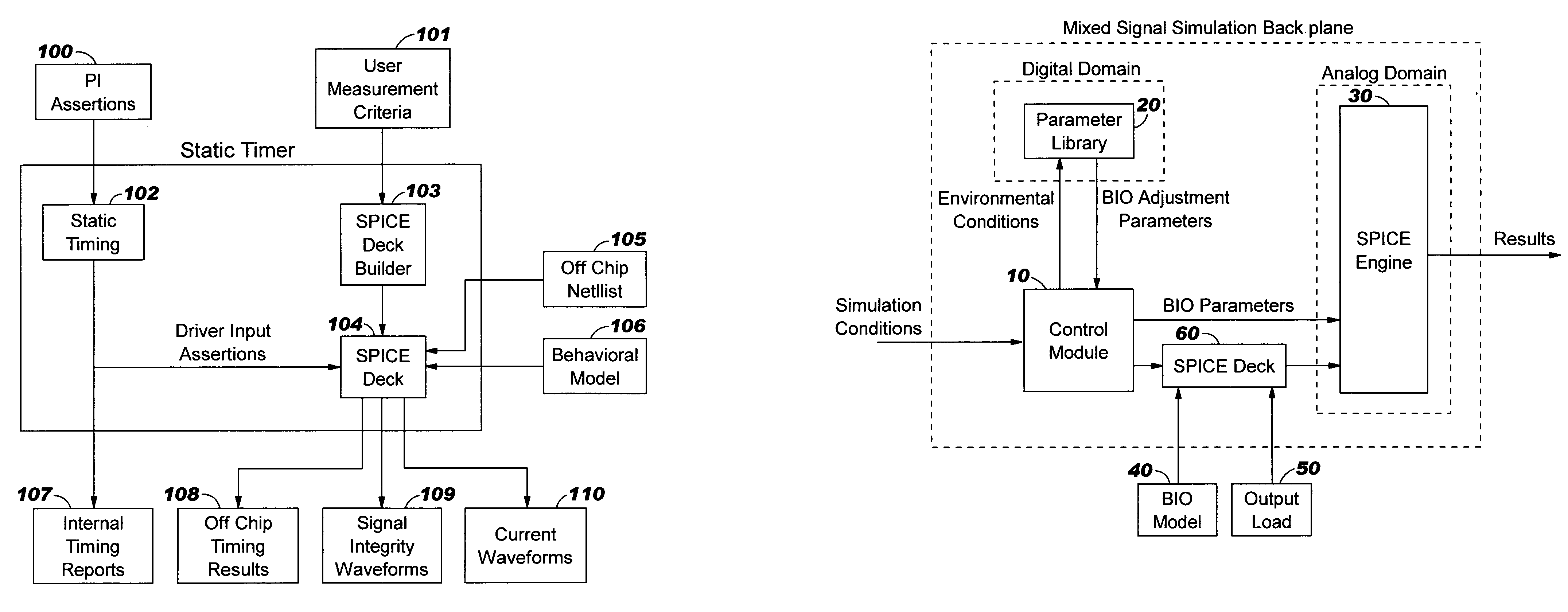
Circuit and method for modeling I/O
a technology applied in the field of circuits and methods for modeling i/o, can solve the problems of pre-drive currents, delay of drivers, and no techniques are available to the ibis model developer to account, and achieve the effect of limiting the cross sectional siz
- Summary
- Abstract
- Description
- Claims
- Application Information
AI Technical Summary
Benefits of technology
Problems solved by technology
Method used
Image

Examples
Embodiment Construction
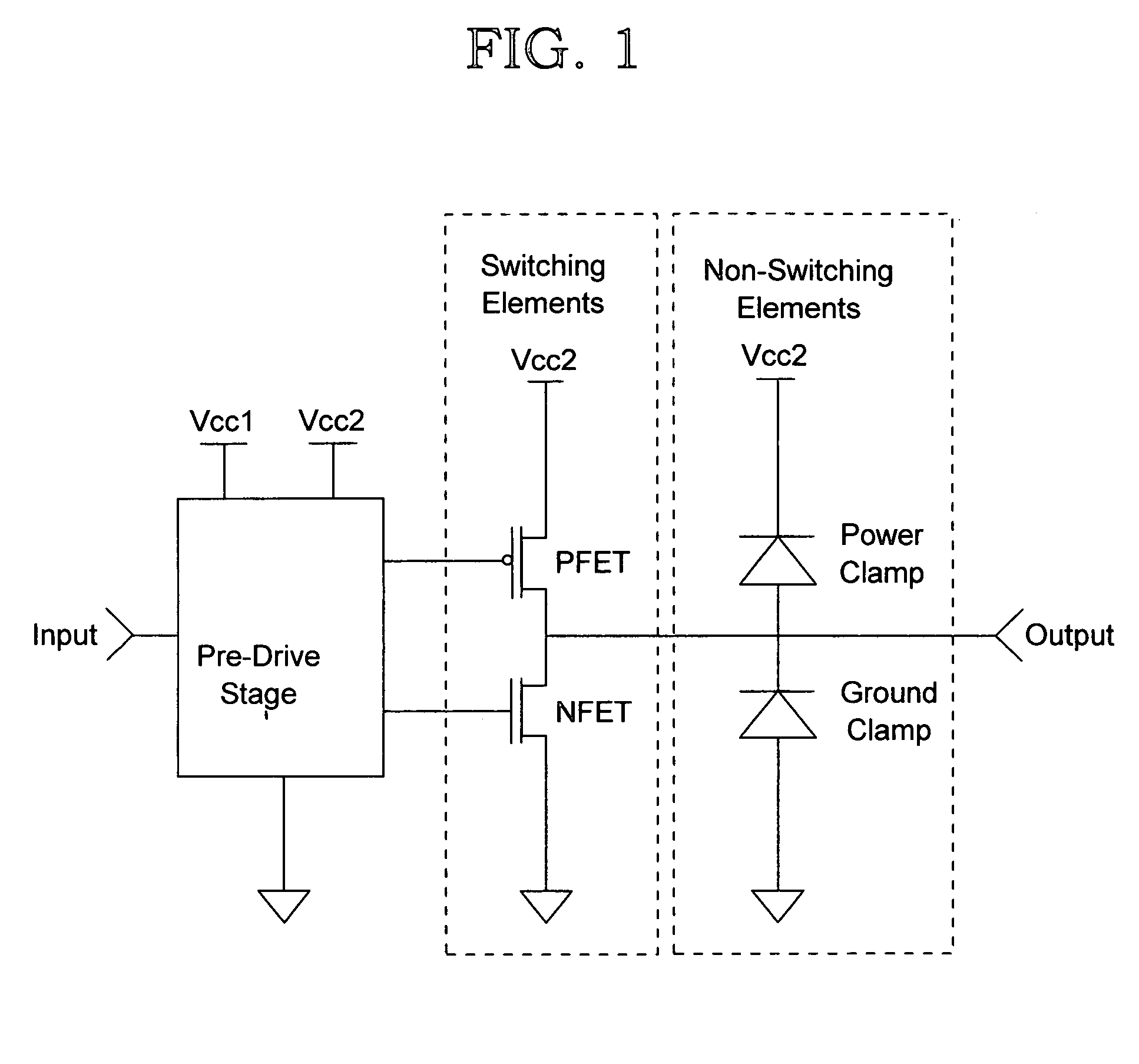
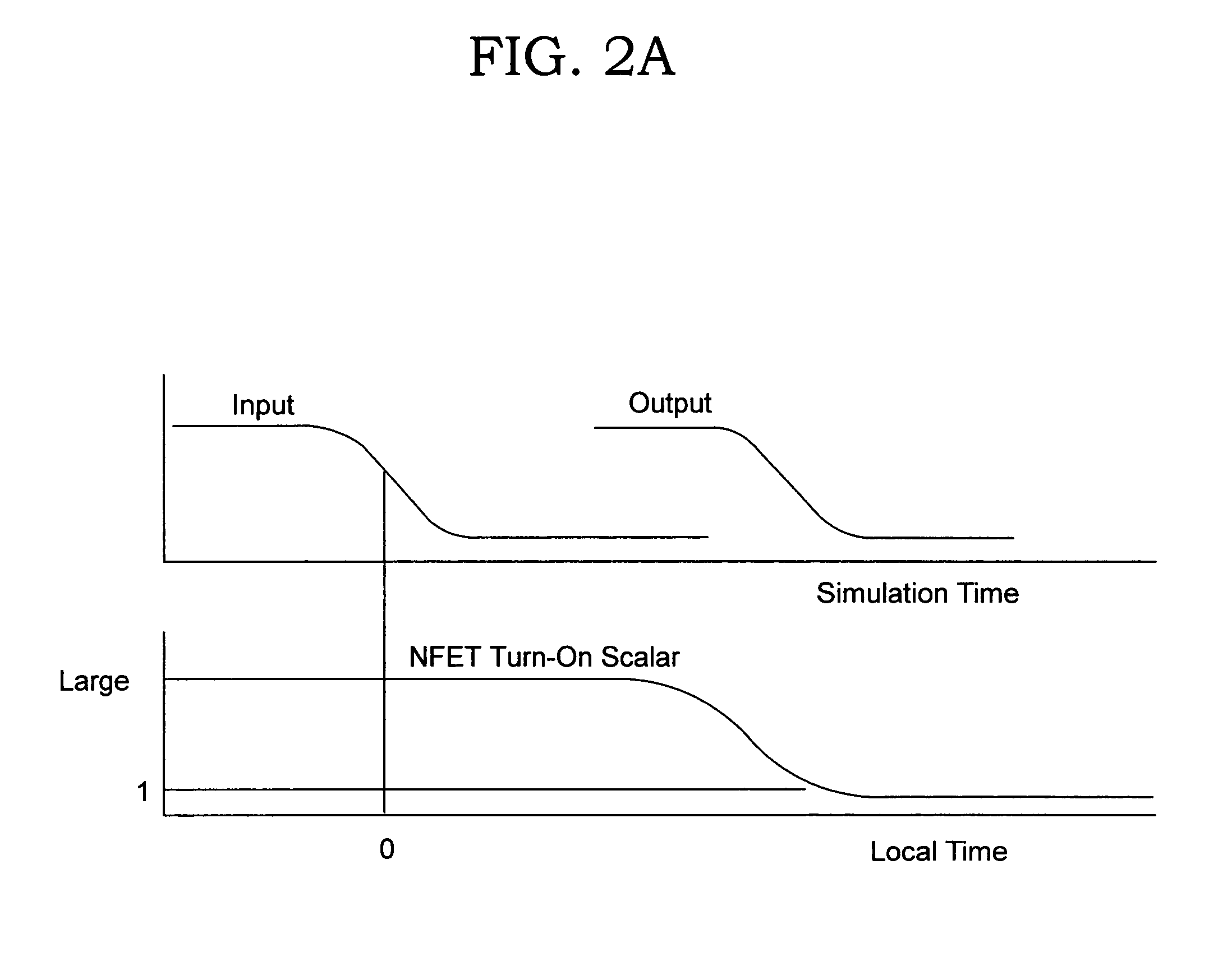
[0029]The output characteristics of a typical driver are represented by two basic element types: switching and non-switching. Switching elements are functions of both time-varying and non-time-varying parameters, and non-switching elements are functions of non-time-varying parameters only. Examples of switching elements are nfets and pfets. Typically, a switching element is used to represent the composite transient impedance (conductance) behavior of a pull-up or pull-down network that are comprised of multiple FETs and parasitics. Examples of non-switching elements are resistive termination's and ESD structures. ESD impedance (conductance) is essentially a function of device voltage only and can therefore can be treated as a non-switching element. There are, however, ESD structures that can be dynamically switched that would require a switching element to represent its impedance.
[0030]FIG. 1 illustrates an example driver structure used to illustrate the characterization techniques ...
PUM
 Abstract
Description
Claims
Application Information