
Switching power supply

a power supply and switch technology, applied in the field of switching power supply, can solve the problems of limiting the application of use, affecting the stability of operation, and not increasing the frequency band of amplified error signals significantly

Inactive Publication Date: 2006-01-10
SHINDENGEN ELECTRIC MFG CO LTD
View PDF14 Cites 26 Cited by
  • Summary
  • Abstract
  • Description
  • Claims
  • Application Information

AI Technical Summary

Benefits of technology

The invention relates to a switching power supply with a control switch, a synchronous switch, and a filter circuit. The control means controls the amplitude of a triangular waveform signal to be between the input of a first comparator and the input of a second comparator. This ensures stable operation of the switching power circuit without the need to lower the frequency band of the error signal. The circuit also includes a current detection circuit and a filter circuit to adjust the output impedance. The invention provides a solution for automatically changing the amplitude of the triangular waveform in response to changes in the load. The control means can be fixed to the clock signal in the steady state, regardless of the load. This ensures stable efficiency and output ripple characteristics. The invention also provides a circuit for automatically changing the amplitude of the triangular waveform in response to changes in the load. The timing of the control switch is fixed to the clock signal in the steady state, regardless of the load. This allows for easy generation of a signal with its phase displaced for multiphasing.

Problems solved by technology

But, due to its poor operational stability, the switching power supply reacts very sensitively against the condition of the output capacitor and the load, limiting its application of usage.
In this mode, operational stability is affected when the frequency difference between the fixed frequency triangular waveform signal and amplified error signal becomes close to zero.
The current mode PWM control means provides an amplified phase allowance for the amplified error signal by using the inductor current signal instead of the fixed frequency triangular waveform signal, but there remains the problem that it can not increase the frequency band of the amplified error signal significantly.
However, as more than few cycles are required to stabilize the output voltage, there was the problem that the response speed of the system delays to obtain stable power supply operation.

Method used


Image

  • Switching power supply
  • Switching power supply
  • Switching power supply

Examples


first embodiment

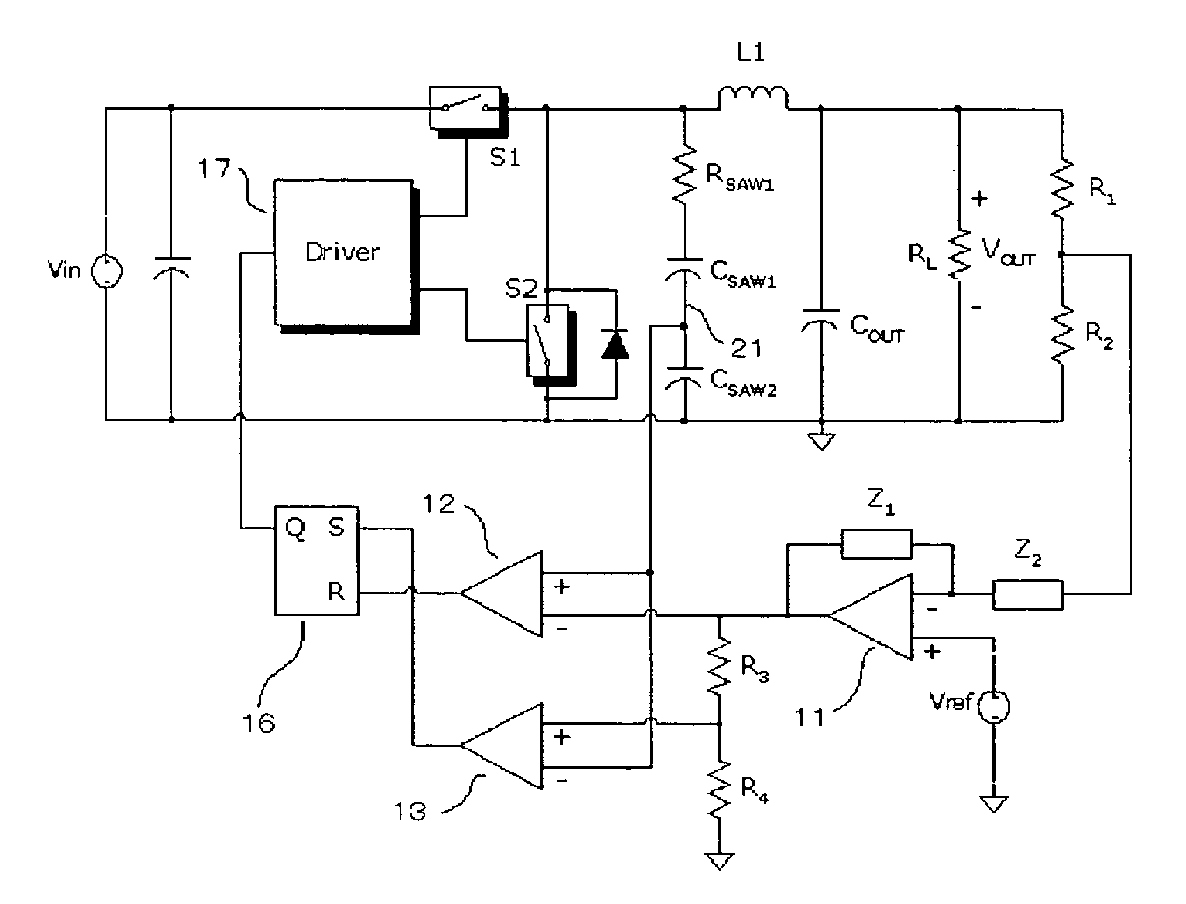
[0090]A switching power supply relating to the invention is describeed below referring to the figures attached hereto. FIG. 1 shows a switching power supply relating to the said embodiment. C represents the capacitor, S the switching element, R the resistor, Z the impedance, 11 the error amplifier, 12 and 13 the comparators, 16 the flip flop circuit, 17 the driver, and 21 the filter circuit.

[0091]The switching power supply relating to this embodiment is provided with control switch S1, synchronous switch S2, output inductor L1, smoothing capacitor Cout, and a power supply circuit in which output inductor L1 and smoothing capacitor Cout are connected in series. A control circuit is connected to the output of said power supply circuit, and its output is connected to control switch S1 and synchronous switch S2.

[0092]Voltage detection resistor R1 and R2 are provided at the output of said power supply circuit, and a connection between resistors R1 and R2 are connected to the negative inp...

third embodiment

[0157]Next, a switching power supply relating to the invention is describeed.

[0158]FIG. 28 shows a switching power supply relating to the said embodiment. C represents the capacitor, S the switching means, R the resistor, Z the impedance, 11 the error amplifier, 12 and 13 the comparators, 36 the current source, 16 the flip flop circuit, 37 the amplifier, 17 the driver, and 21 the filter circuit.

[0159]The switching power supply relating to said embodiment is provided with control switch S1, synchronous switch S2, output inductor L1, smoothing capacitor Cout, and a power supply circuit connected in series to output inductor L1 and smoothing capacitor Cout1. The output of said power supply circuit is connected to a control circuit, the output of which is connected to control switch S1 and synchronous switch S2.

[0160]The switching power supply is provided with resistors for voltage detection R1 and R2 at the output of the power supply circuit, and a connection between said resitors is c...

fourth embodiment

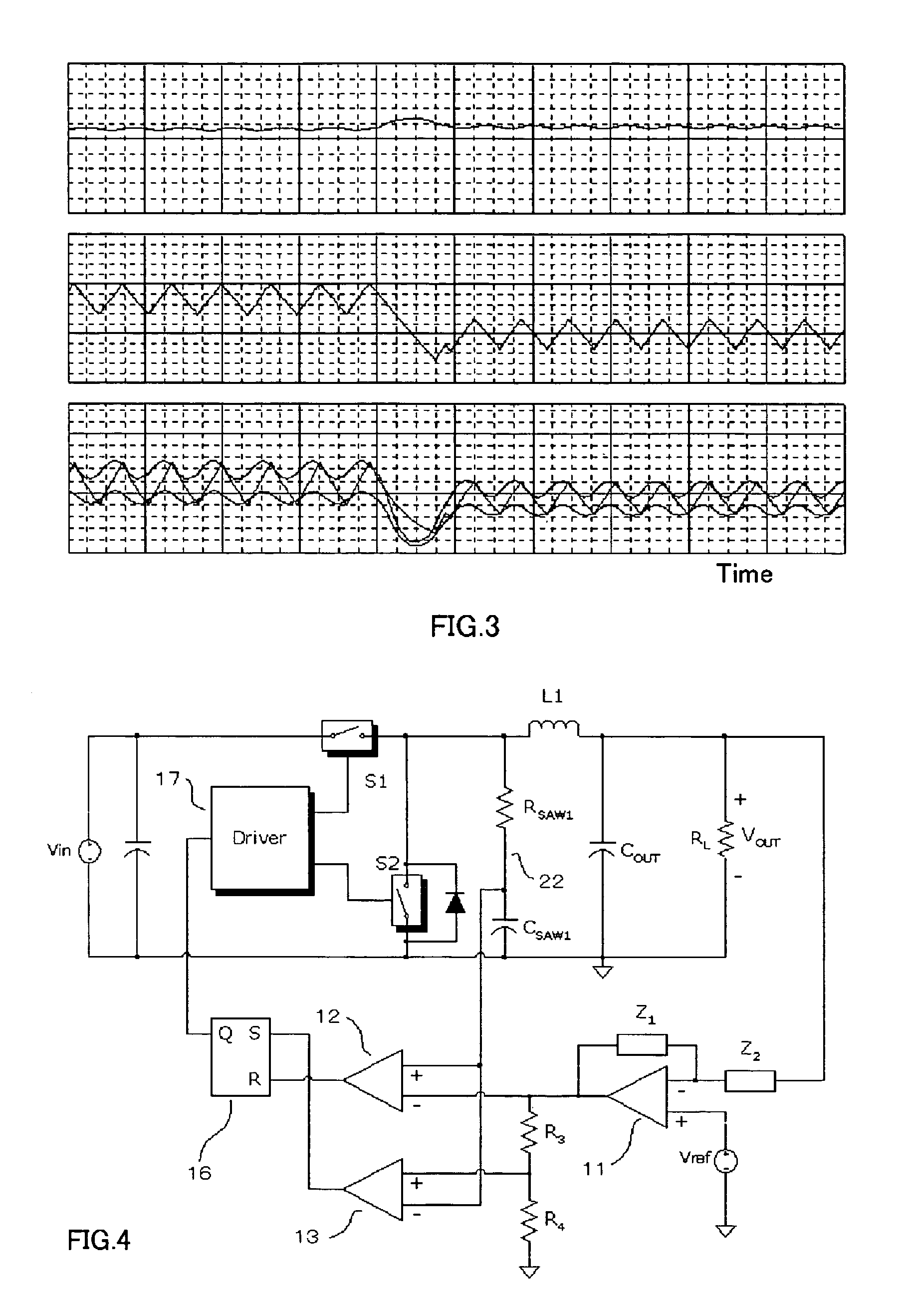
[0189]Next, a switching power supply relating to the invention is described. FIG. 42 shows a switching power supply relating to said embodiment. C represents capacitor, S the switching device, R the resistor, Z the impedance, 11 the error amplifier, 12 and 13 the comparators, 39 the OR circuit, 16 the flip flop circuit, 17 the driver, and 21 the filter circuit.

[0190]The switching power supply relating to this embodiment is provided with control switch S1, synchronous switch S2, output inductor L1, capacitor Cout, and a power supply circuit in which output inductor L1 and smoothing capacitor Cout are connected in series. The output of—said power supply circuit is connected to a control circuit, the output of which is connected to control switch S1 and synchronous switch S2.

[0191]Resistors R1 and R2 for voltage detection are provided at the output of the the power supply circuit, and a connection between said resistors is connected to the negative input of error amplifier 11 which amp...


PUM


Abstract

A switching power supply; wherein a voltage detector is provided at the output of a power supply circuit and connected to the negative input of an error amplifier to amplify the error between detected voltage and reference voltage, the output of said amplifier is connected to the negative input of a first comparator and to the negative input of a second comparator through split resistors, a filter circuit is connected between a control switch and synchronous switch and the output of said filter circuit is connected to a first comparator and a second comparator, wherein said configuration constitues a control means to control the amplitude of the triangular waveform obtained through said filter circuit to be between an input level of said first comparator and an input of said second comparator, whereby the stability of the switching power supply is ensured without lowering the frequency band of said amplified error signal and stable output ripple characteristics can be materialized.

Description

TECHNICAL FIELD[0001]This invention relates to a switching power supply provided with a control means which improves the response speed against a sharp change of the load.BACKGROUND ART[0002]Existing switching power supplies are shown in FIG. 60 to FIG. 62. The switching power supply shown in FIG. 60 is provided with a voltage hysteresis control means. More particularly, the output of the power supply circuit is connected to the negative input of comparator 42 to amplify the error between detected voltage and reference voltage Vref. The output of comparator 42 is connected to the input of driver 47, the output of which is connected to the gate of control switch S1 and the gate of synchronous switch S2 (for example, refer to FIG. 3 in Section 7 of U.S. Pat. No. 6,147,478). A switching power supply shown in FIG. 61 is provided with a voltage mode PWM control means. More particularly, the output of said power supply circuit is connected to the negative input of error amplifier 41 to am...

Claims


Application Information

Patent Timeline
Patent Type & Authority Patents(United States)
IPC IPC(8): G05F1/40H02M3/156H02M3/158
CPCH02M3/156H02M3/1588Y02B70/1466Y02B70/10H02M3/155
Inventor KUBOTA, KENICHISUZUKI, KENICHISEKINE, YUTAKAOSHIMA, MASAKIWATANABE, HARUOHAGA, HIROYUKIKIKUCHI, YOSHIHIKOHAYASHI, MASANORIZENTA, KENICHINOZAKI, YUKIHIRO
Owner SHINDENGEN ELECTRIC MFG CO LTD
Learn More