Inkjet head for inkjet printing apparatus having pressure chambers and actuator unit
a technology of inkjet printing and actuator unit, which is applied in the direction of printing and inking apparatus, etc., can solve the problem that the type of inkjet head described in the above-mentioned patent is insufficient to meet such a demand
- Summary
- Abstract
- Description
- Claims
- Application Information
AI Technical Summary
Benefits of technology
Problems solved by technology
Method used
Image
Examples
concrete examples
[0067]Hereinafter, concrete examples of the inkjet heads according to the embodiment, and comparative examples will be described.
first concrete example
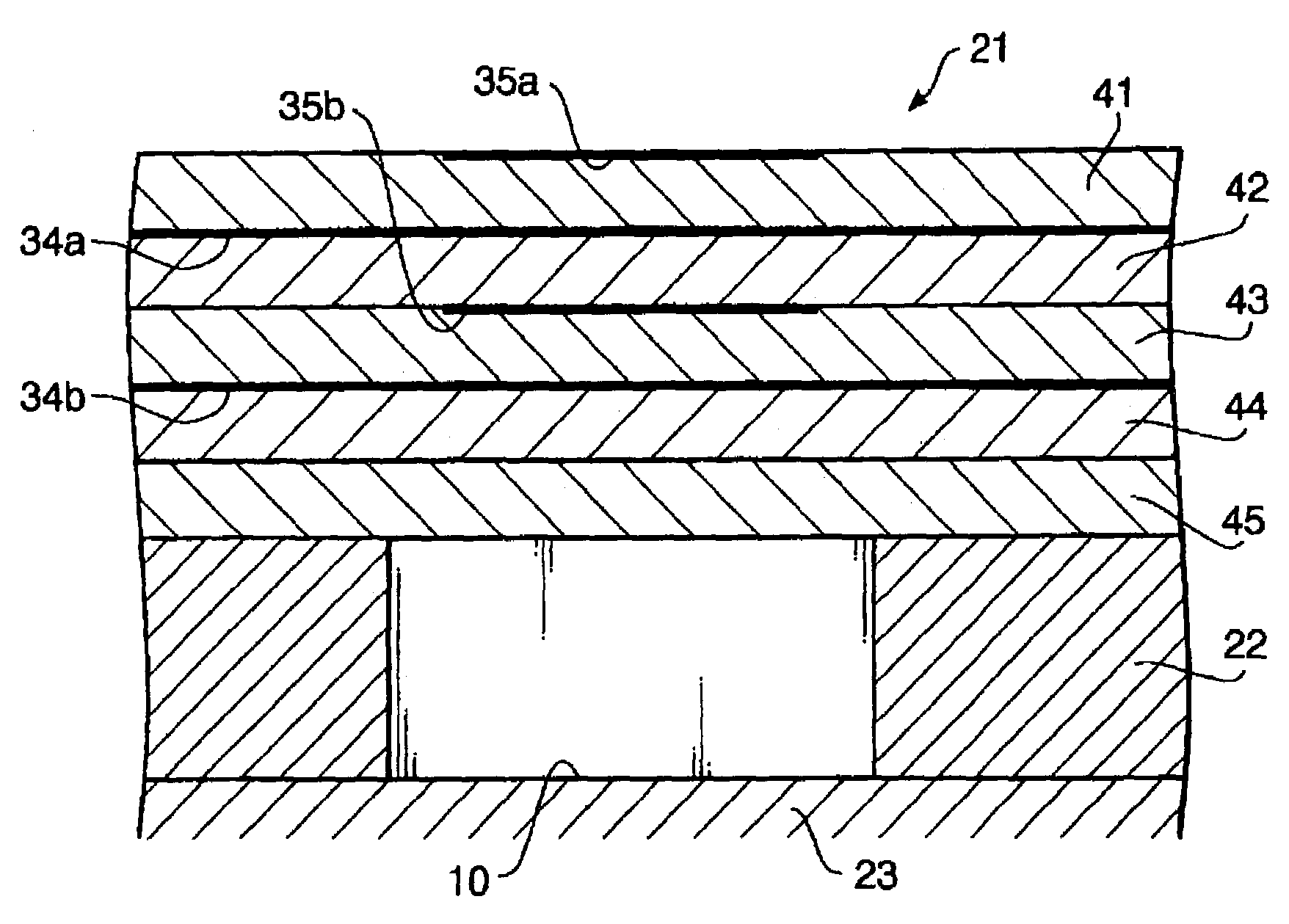
[0068]In the first concrete example, the active layers, the inactive layers and the pressure chambers are located in this order from the top to the bottom.
[0069]The electrical efficiency and area efficiency are obtained by simulation for an inkjet head which has a structure similar to the above-described structure except that there are two active layers (width of the driving electrodes are 200 μm), and two inactive layers. The thickness of each of the active and inactive layers is 15 μm. The result is shown in TABLE 1. The simulation is performed such that a pressure corresponding to the maximum pressure in the pressure chamber is applied to the entire bottom surface of the piezoelectric element (the following simulations are performed similarly).
Second and Third Concrete Examples
[0070]The electric efficiency and area efficiency are obtained by simulation for an inkjet head which is manufactured in the same manner as that of the inkjet head 1 of the concrete first example except tha...
fourth through seventh
Concrete Examples
[0071]The electric efficiency and area efficiency are obtained by simulation for an inkjet head which has an arrangement similar to that of the above-described embodiment except that there are three active layers (Example 4: the width of the driving electrode on the top layer is 250 μm and those of the other two driving electrodes are 300 μm, Example 5: the width of the driving electrode on the top layer is 200 μm and those of the other two driving electrodes are 300 μm, Example 6: the width of each driving electrode is 300 μm, Example 7: the width of the driving electrode on the top layer is 150 μm and those of the other two are 300 μm), and two inactive layers. The thickness of each active and inactive layers is 15 μm. The result is shown in table 1.
PUM
 Abstract
Description
Claims
Application Information


