Check patentability & draft patents in minutes with Patsnap Eureka AI!

Surface preparation for receiving processing treatments

Active Publication Date: 2006-01-24
S O I TEC SILICON ON INSULATOR THECHNOLOGIES
View PDF12 Cites 14 Cited by
  • Summary
  • Abstract
  • Description
  • Claims
  • Application Information

AI Technical Summary

Benefits of technology

[0014]The invention relates to a method for preparing a surface of a semiconductor wafer which comprises polishing the wafer surface with a polishing solution that includes dispersed solid particles for mechanically abrading the wafer surface and a chemical agent for chemically attacking the wafer surface, with the polishing conducted to obtain planarization of the wafer surface; and controllably stopping the chemical attack of the wafer surface by progressively introducing a rinsing solution onto the wafer surface to prevent chemical attack of the wafer surface beyond a desired planarization.
[0015]Advantageously, the polishing solution has a basic pH and the rinsing solution has an acidic pH, so that the progressive introduction of the rinsing solution changes the pH of the polishing solution to terminate the chemical attack of the chemical agent on the wafer surface.

Problems solved by technology

Further erosion of the surface may be undesirable because precise control over the thickness of the planarized object is sometimes required.
Such techniques can often reduce the rate of production of polished wafers because the duration used for rinsing needs to be long enough to allow the polishing residues to be properly removed.
This aspect is often detrimental in the industrial context.
One drawback of the use of such additives is that their use tends to continue the polishing action.
Other drawbacks may additionally exist in the context of silicon-on-insulator type structures in which a thin layer of a substantially metal-free material containing silicon is subject to such CMP processes.
Since the top layer in such structures is already thin even before polishing, the available range of tolerance the thickness of the layer can be decreased is relatively limited.
This may be because large-sized grit particles (e.g., around 1 micron) that are used in the CMP process of metal surfaces such as, a tungsten surface, may not be underestimated when compared with the erosion caused by the chemical etchants.
In this context, however, the grit particles may also cause damage to the surface being polished (e.g., scratches or holes) because of their considerable size.
Since, the effect of the grit particles is less dominant in the “non-metallic” wafer context, the use of a surfactant in the polishing solution to curb the aggressiveness of the grit particles is of less concern and may disadvantageously increase production costs with little realized benefit to the end product.
Another drawback, is that the use of the surfactant will reduce productivity because it will slow the effect of the chemical agent in the polishing solution.
This may substantially increase the wafer polishing time (e.g., increase by a factor of ten) and reduce the productivity of the fabrication line.

Method used


Image

  • Surface preparation for receiving processing treatments
  • Surface preparation for receiving processing treatments
  • Surface preparation for receiving processing treatments

Examples


Embodiment Construction

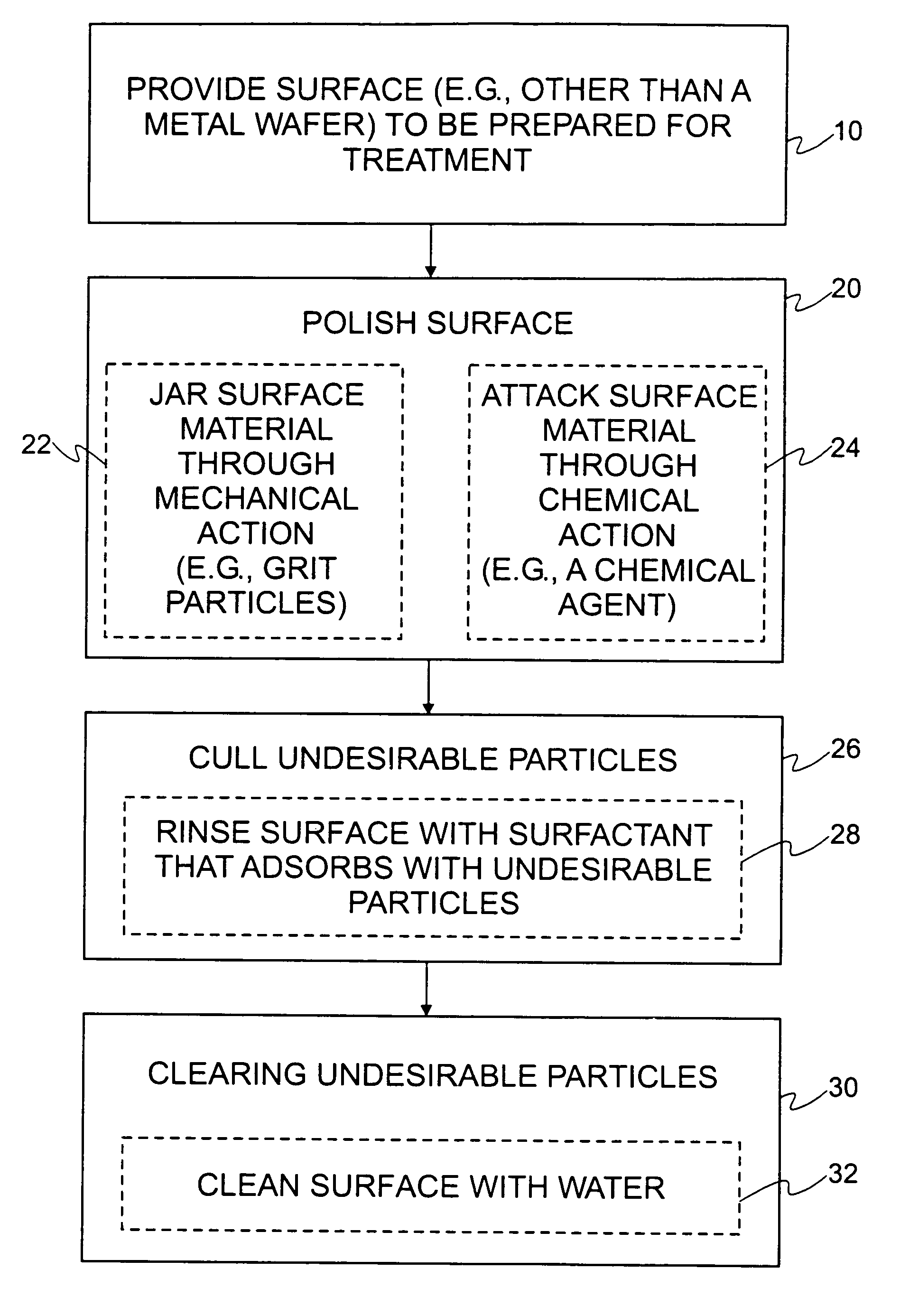
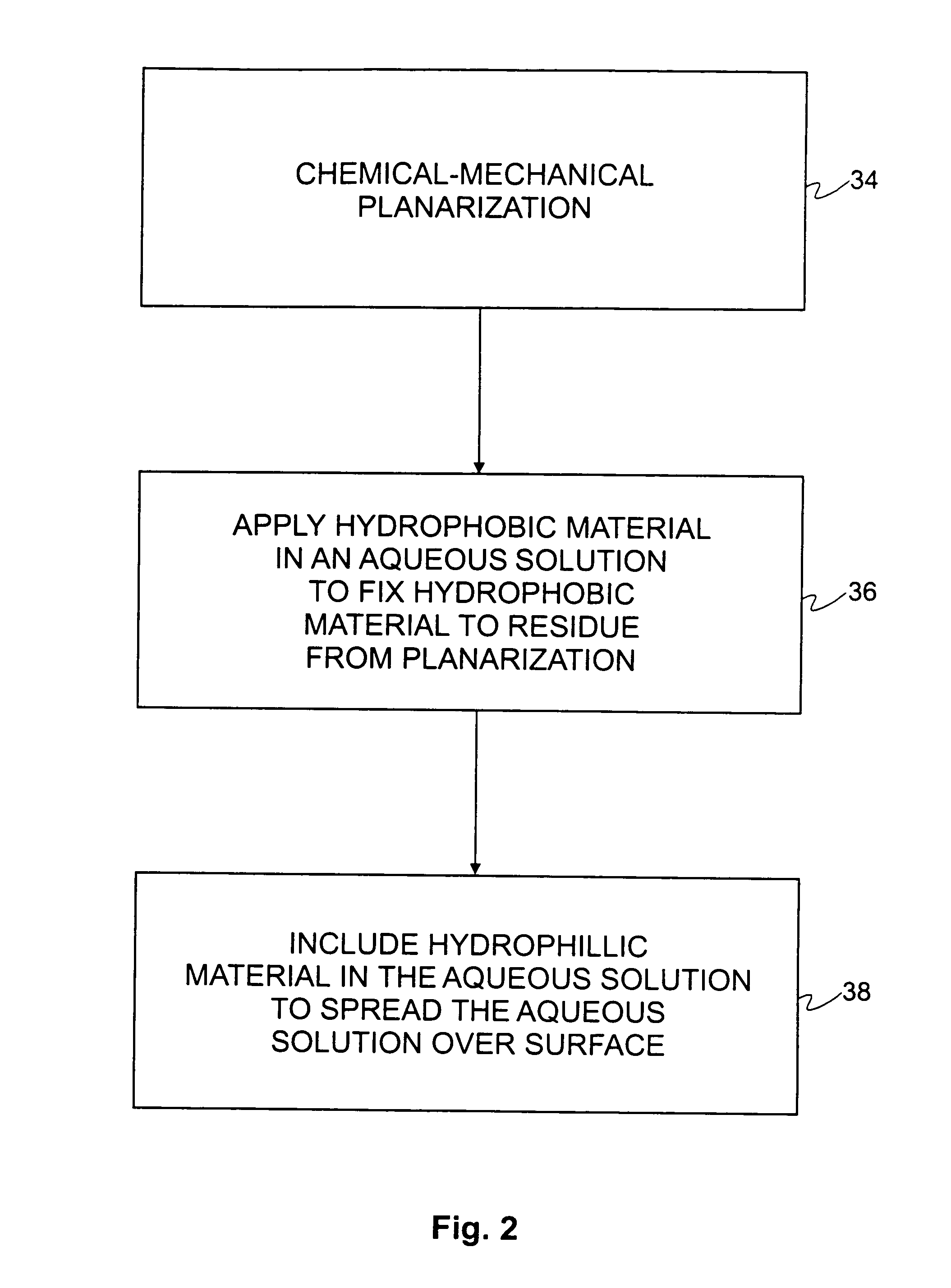
[0025]In accordance with the principles of the present invention, CMP type processing techniques involving rinsing surfaces with a surfactant solution may be provided. Surfaces such as a “non-metallic” surface of a wafer may be subject to such CMP type processing techniques. Such surfaces may, for example, include a wafer surface of a semiconductor material layer or other layer having material which is capable of hosting an integrated circuit component formed from treatment of the material (e.g., oxidation, doping, etching). A surface may be rinsed with a rinsing solution that acts to clear undesirable particles and to end “latent” polishing action.

[0026]Polishing may include using a polishing solution that includes particles for causing mechanical action on a surface being polished and include a chemical agent for chemical attack of the surface. Polishing may be performed to correct surface roughness. A polishing plate, which may be covered with a textured material such as a fabric...


PUM

PropertyMeasurementUnit
Fractionaaaaaaaaaa
Thicknessaaaaaaaaaa
Critical micelle concentration (mass)aaaaaaaaaa

Abstract

A solution for rinsing a surface that has been planarized using a chemical-mechanical planarization (“CMP”) technique. The solution may be a surfactant solution introduced following the use of a polishing solution in the CMP technique. The surfactant solution acts to clear undesirable particles from the planarized surface and also can terminate “latent” effects from the polishing solution. A cleaning solution is generally injected after the rinsing solution for additional cleaning effects. A plate covered with a textured material such a fabric is usually applied to the surface during the polishing, rinsing, or cleaning steps.

Description

CROSS-REFERENCE TO RELATED PATENT APPLICATION[0001]This application claims the benefit of U.S. Provisional Application No. 60 / 446,985, filed Feb. 12, 2003, which application is hereby incorporated herein in its entirety by reference thereto.BACKGROUND[0002]The present invention relates generally to preparing a wafer for processing treatments, and more specifically, relates to configuring a wafer surface to receive active integrated circuit components via semiconductor processing treatments.[0003]Typically, planarization of a wafer surface is performed to suitably prepare the wafer surface for treatment in which the wafer surface is used to guild integrated circuit components (e.g., a transistor). In some known techniques, planarization is conducted through chemical and mechanical action. In chemical-mechanical planarization (“CMP”) techniques, the surface of a wafer is polished using a polishing solution and a polishing plate, which is typically shaped in the form of disc. A chemica...

Claims


Application Information

Patent Timeline
IPC IPC(8): B24B1/00H01L21/304B08B1/04B24BB24B7/22B24B37/04B28D5/00H01L21/02H01L21/306
CPCB24B37/0056H01L21/30625H01L21/02052B24B37/042H01L21/02024
Inventor FILIPOZZI, LAURENTMETRAL, FREDERIC
Owner S O I TEC SILICON ON INSULATOR THECHNOLOGIES
Features
  • R&D
  • Intellectual Property
  • Life Sciences
  • Materials
  • Tech Scout
  • Unparalleled Data Quality
  • Higher Quality Content
  • 60% Fewer Hallucinations
Learn More