Driving of a liquid crystal display device
a liquid crystal display and active matrix technology, applied in static indicating devices, non-linear optics, instruments, etc., can solve the problems of low-voltage liquid crystal, particularly vulnerable to contamination, and tends to occur images sticking,
- Summary
- Abstract
- Description
- Claims
- Application Information
AI Technical Summary
Benefits of technology
Problems solved by technology
Method used
Image
Examples
first embodiment
[First Embodiment]
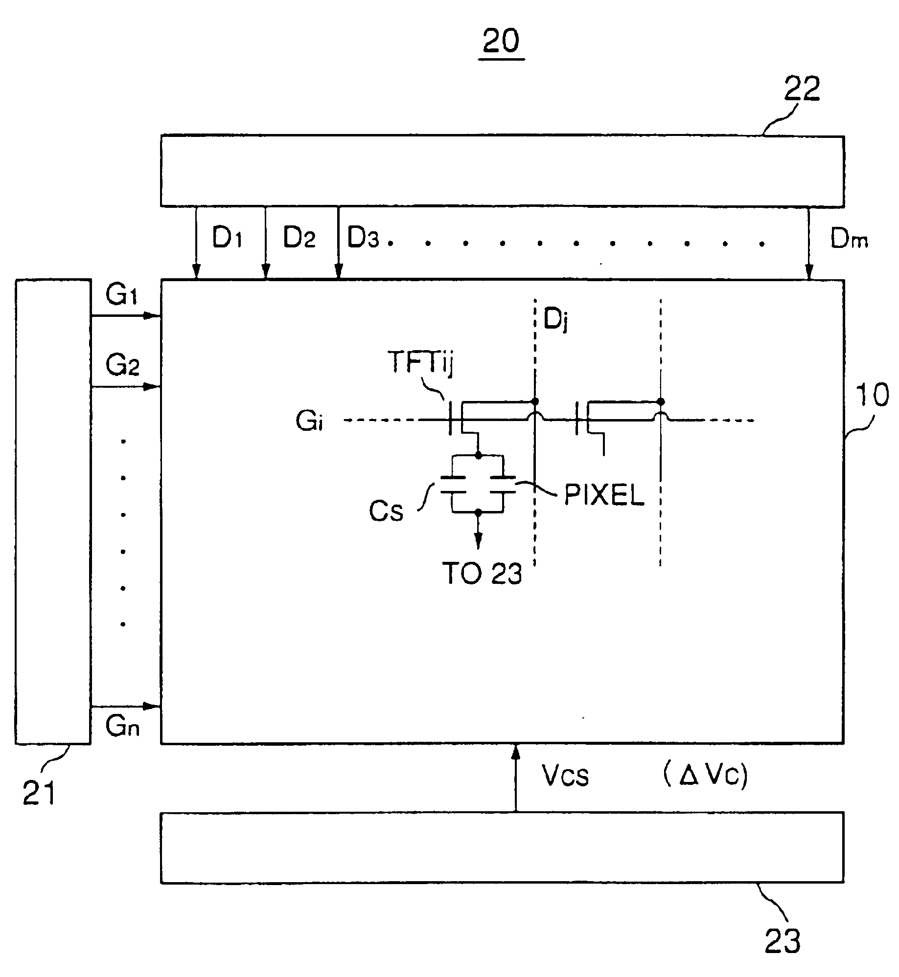
[0036]FIG. 5 shows the construction of a liquid crystal display device 20 according to a first embodiment of the present invention, wherein those parts corresponding to the parts described previously are designated by the same reference numerals and the description thereof will be omitted.
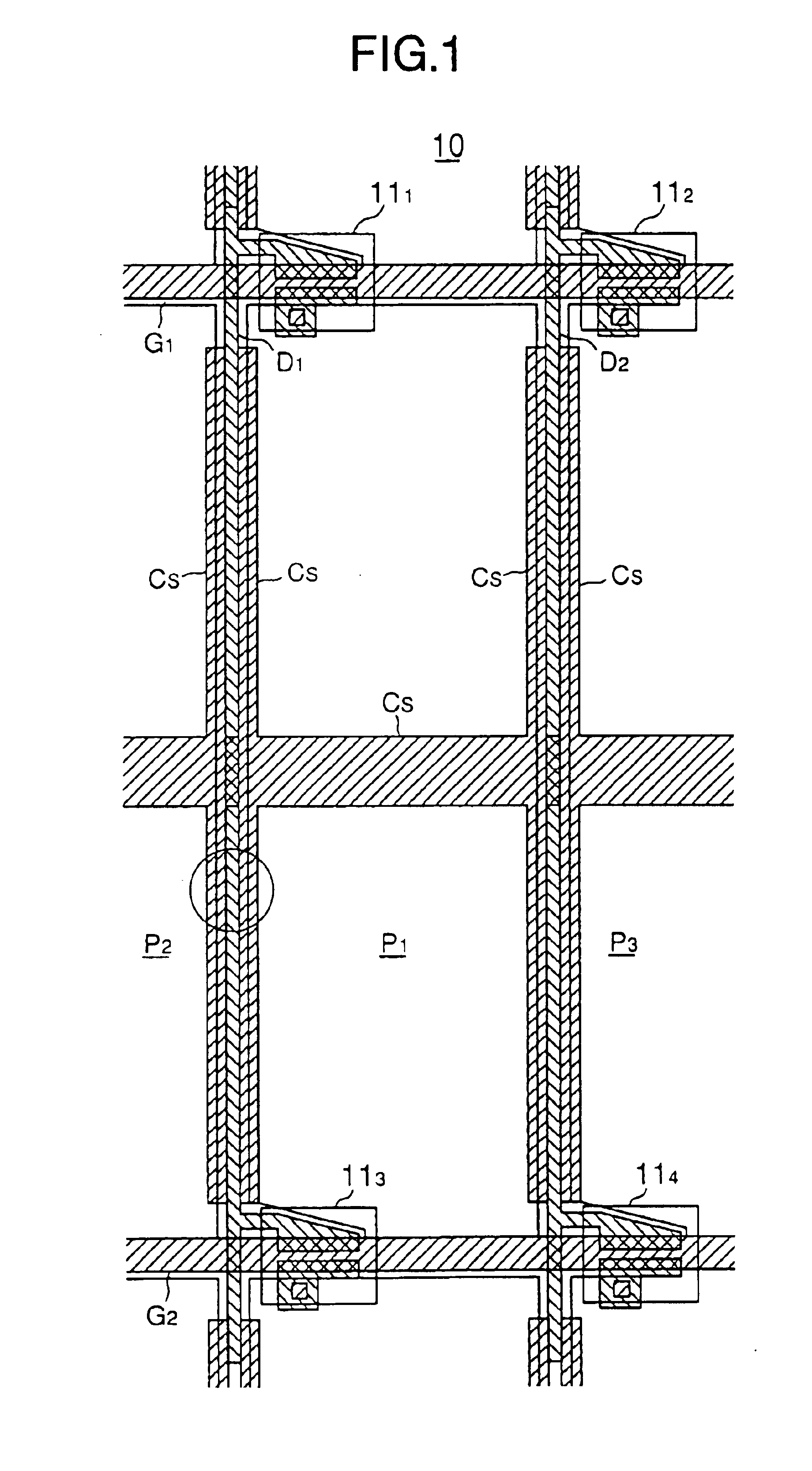
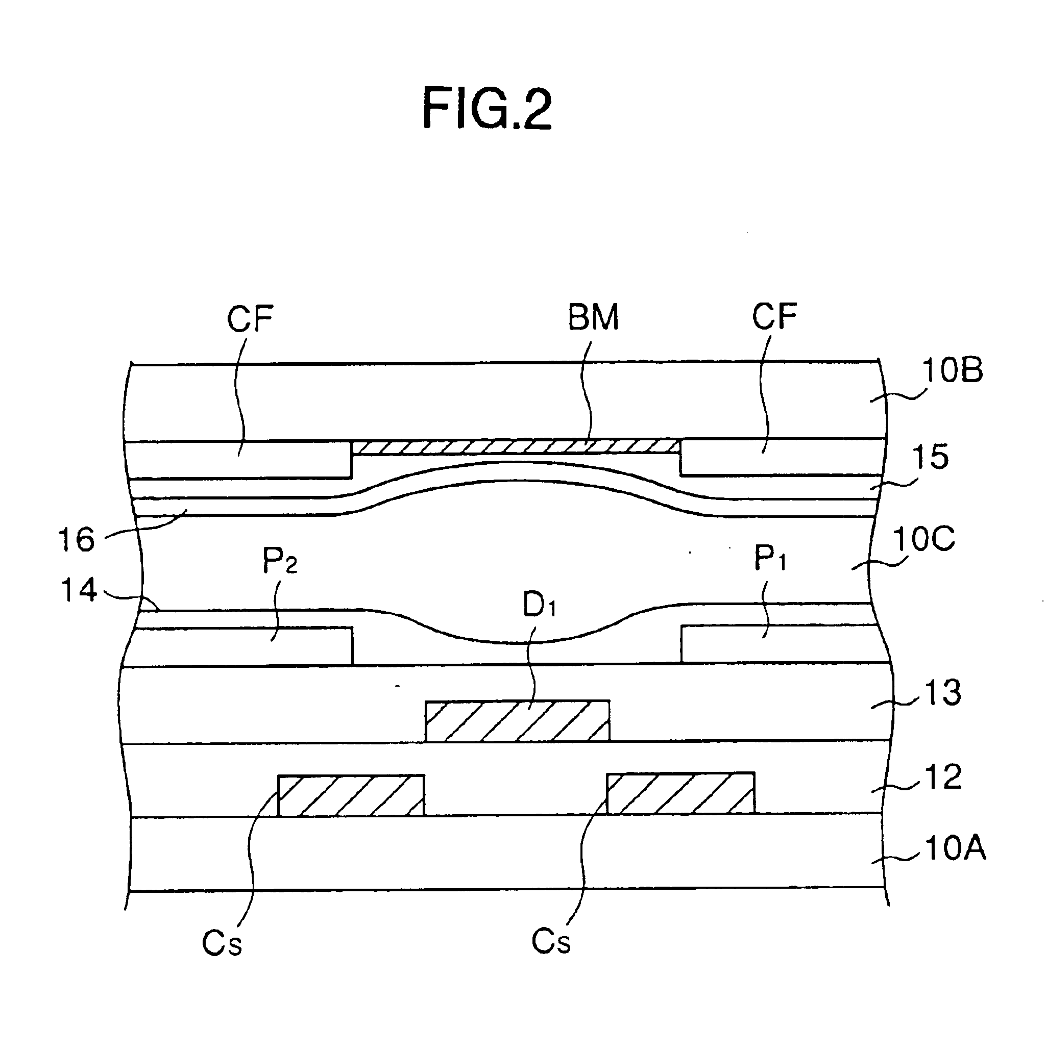
[0037]Referring to FIG. 5, the liquid crystal display device 20 includes, in addition to the liquid crystal panel 10 described previously with reference to FIGS. 1 and 2, a scanning-electrode driving circuit 21 for selectively activating the gate bus lines G1-Gn and a signal electrode driving circuit 22 for supplying the A.C. driving signal explained with reference to FIG. 3 to the data bus lines D1-Dm, and there is further provided a D.C. voltage source 23 supplying the common voltage VCs to the opposing electrode 15 and to the auxiliary electrode Cs as a common voltage supply source. FIG. 5 further indicates a capacitor PIXEL, wherein it should be noted that the capacitor PIXEL ...
second embodiment
[Second Embodiment]
[0048]In the foregoing embodiment, it was assumed that the drive voltage pulse signal supplied to the data bus lines D1-Dm is a bipolar voltage pulse having a central voltage of 0V. The present invention, however, is never limited to such a particular driving signal but is applicable to the case in which the driving voltage pulse signal includes a D.C. voltage offset as represented in FIG. 8.
[0049]Referring to FIG. 8, the driving voltage pulse signal has a voltage amplitude of ±2.5V in the black representation mode, and the driving voltage pulse signal is supplied to the data bus line D1-Dm together with a D.C. offset of 2.37V. Thereby, an optimum common voltage VCs of 2.37V, which is substantially equal to the foregoing D.C. voltage offset, is applied to the auxiliary electrode Cs and to the opposing electrode 15.
[0050]In the driving process noted above, it should be noted that the optimum common voltage VCs may be different in the black representation mode and i...
PUM
| Property | Measurement | Unit |
|---|---|---|
| central voltage | aaaaa | aaaaa |
| voltage | aaaaa | aaaaa |
| drive voltage VD | aaaaa | aaaaa |
Abstract
Description
Claims
Application Information


