Ultra-thin, high quality strained silicon-on-insulator formed by elastic strain transfer

a silicon-on-insulator, elastic strain transfer technology, applied in the direction of basic electric elements, electrical equipment, semiconductor devices, etc., can solve the problems of high vlsi (very large scale integration) applications, thick sige buffer layers are not typically easy to integrate with existing si-based cmos technology, and circuits employing devices with strained si

Inactive Publication Date: 2006-01-31
GLOBALFOUNDRIES INC
View PDF90 Cites 101 Cited by
  • Summary
  • Abstract
  • Description
  • Claims
  • Application Information

AI Technical Summary

Benefits of technology

[0006]The present invention provides a method for fabricating a thin (less than 500 Å) first semiconductor layer that is mechanically strained in a tensile or compressive manner over an insulating layer, which, in turn, exists on a semiconductor substrate. Specifically, the method of the present invention allows for the formation of a strained semiconductor-on-insulator (SSOI) heterostructure, without the presence of SiGe in the final structure.
[0008]The annealing step of the present invention is performed in such a way as to minimize the amount of Ge diffusion into the first semiconductor layer. After the annealing step, the stress-providing layer is selectively removed at a temperature below the reflow temperature of the buried insulating layer. The reflow temperature of the buried insulating layer can be controlled in the present invention to some extent by doping it with different elements. For example, boron can be used as a dopant species to reduce the reflow temperature of the buried insulating layer. After removing the stress-providing layer, what remains is a thin, strained (tensile or compressive) first semiconductor layer (less than 500 Å) atop the buried insulating layer of the substrate.

Problems solved by technology

Despite the high channel electron mobilites reported for prior art heterostructures, the use of thick SiGe buffer layers has several noticeable disadvantages.
First, thick SiGe buffer layers are not typically easy to integrate with existing Si-based CMOS technology.
Second, the defect densities, including threading dislocations (TDs) and misfit dislocations (MDs) are from about 106 to about 108 defects / cm2 which are still too high for realistic VLSI (very large scale integration) applications.
Thirdly, the nature of the prior art structures precludes selective growth of the SiGe buffer layer so that circuits employing devices with strained Si, unstrained Si and SiGe materials are difficult, and in some instances, nearly impossible to integrate.

Method used


Image

  • Ultra-thin, high quality strained silicon-on-insulator formed by elastic strain transfer
  • Ultra-thin, high quality strained silicon-on-insulator formed by elastic strain transfer
  • Ultra-thin, high quality strained silicon-on-insulator formed by elastic strain transfer

Examples


Embodiment Construction

[0018]The present invention, which provides a method of fabricating a strained semiconductor-on-insulator (SSOI) heterostructure as well as a low-defect density (SFs and TDs) SSOI heterostructure produced by the inventive method, will now be described in greater detail by referring to the drawings that accompany the present application. The accompanying drawings, which are not drawn to scale, are provided for illustrative purposes only and like and / or corresponding elements referred to in the drawings are described with respect to like reference numerals.

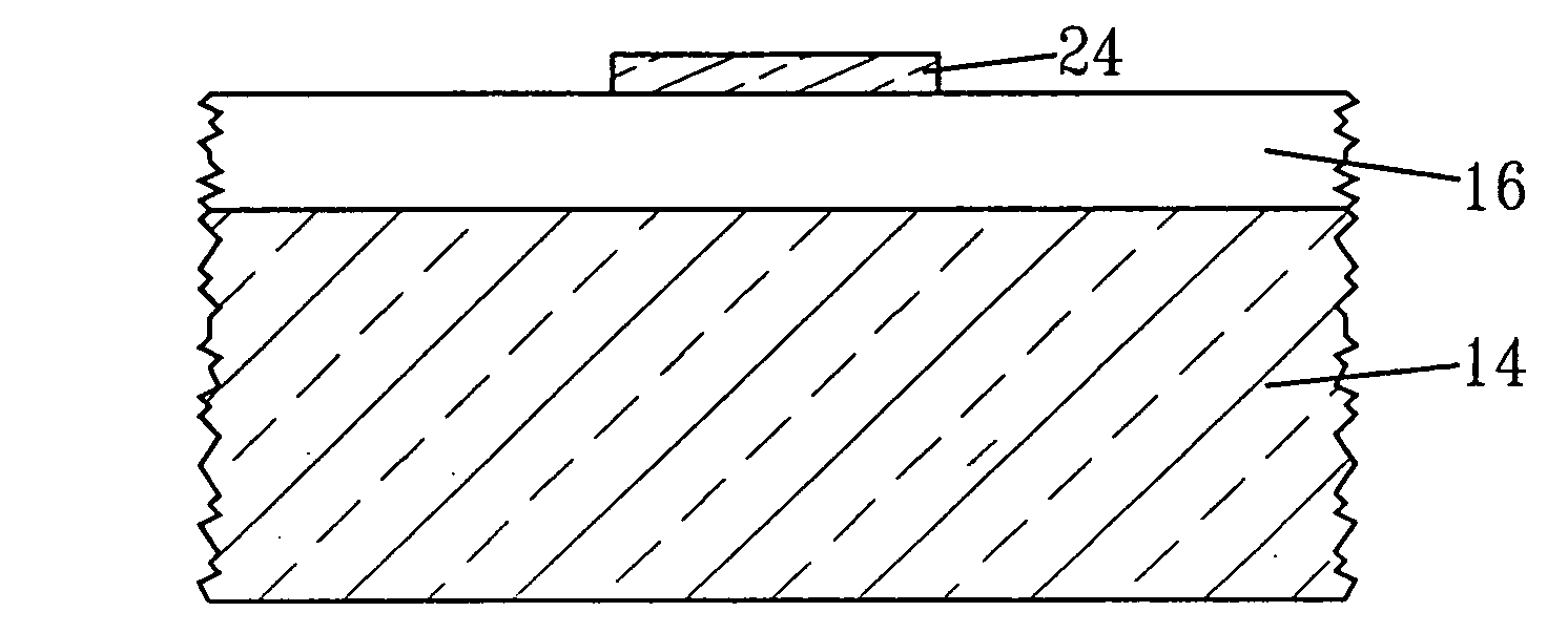
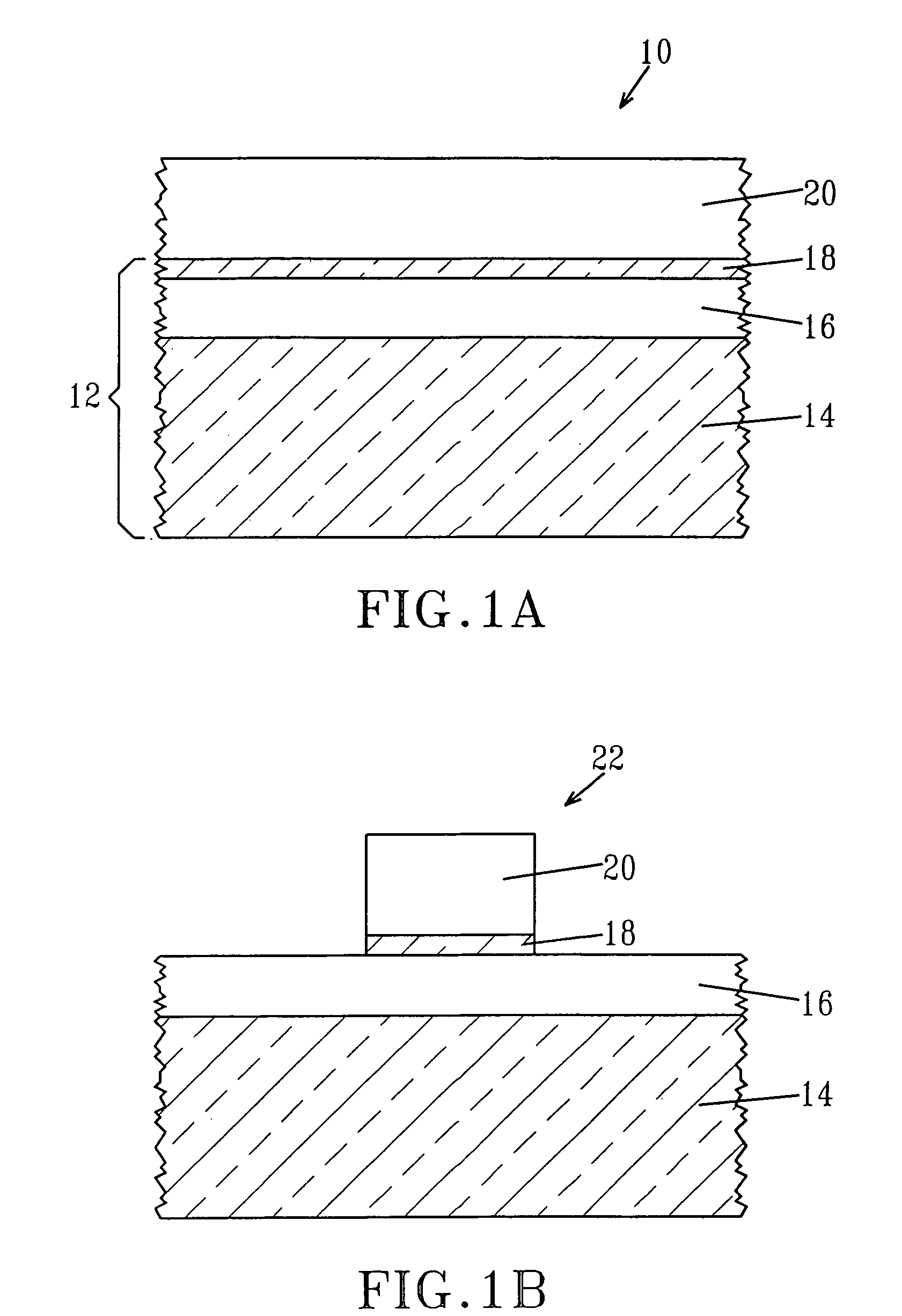
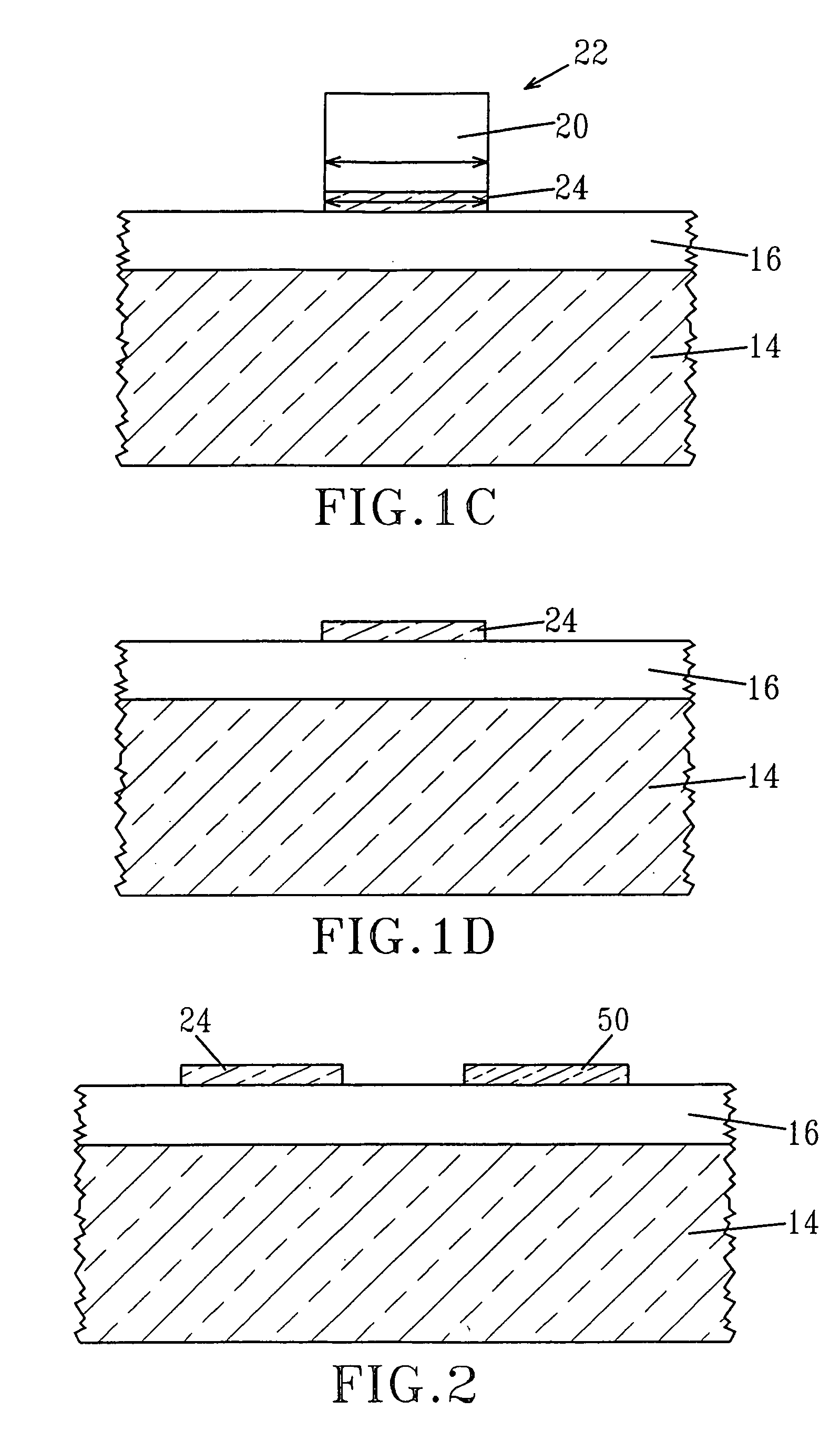
[0019]The VEST process begins with first providing a layered structure 10 such as shown in FIG. 1A. Layered structure 10 includes a semiconductor substrate 12 having a stress-providing layer 20 located on an upper surface thereof. The semiconductor substrate 12 includes a bottom semiconductor layer 14, a buried insulating layer 16 and a top semiconductor layer 18 (hereinafter referred to as the first semiconductor layer).

[0020]In th...


PUM


Abstract

A method of forming a semiconductor structure comprising a first strained semiconductor layer over an insulating layer is provided in which the first strained semiconductor layer is relatively thin (less than about 500 Å) and has a low defect density (stacking faults and threading defects). The method of the present invention begins with forming a stress-providing layer, such a SiGe alloy layer over a structure comprising a first semiconductor layer that is located atop an insulating layer. The stress-providing layer and the first semiconductor layer are then patterned into at least one island and thereafter the structure containing the at least one island is heated to a temperature that causes strain transfer from the stress-providing layer to the first semiconductor layer. After strain transfer, the stress-providing layer is removed from the structure to form a first strained semiconductor island layer directly atop said insulating layer.

Description

RELATED APPLICATIONS[0001]This application is related to co-pending and co-assigned U.S. patent application Ser. No. 10 / 300,189, filed Nov. 20, 2002, entitled “Relaxed Low-Defect SGOI For Strained Si CMOS Applications”. The entire content of the aforementioned U.S. Patent Application is incorporated herein by reference.FIELD OF THE INVENTION[0002]The present invention relates to a method of fabricating a semiconductor structure that can be used as a substrate for high performance complementary metal oxide semiconductor (CMOS) devices, and more particularly to a method of creating a first strained semiconductor layer over an insulating layer. Even more particularly, the present invention provides a method of forming a strained semiconductor-on-insulator (SSOI) substrate material.BACKGROUND OF THE INVENTION[0003]In the semiconductor industry, there has recently been a high-level of activity using strained Si-based heterostructures to achieve high carrier mobility structures for comple...

Claims


Application Information

Patent Timeline
Patent Type & Authority Patents(United States)
IPC IPC(8): H01L21/20
CPCH01L29/78696H01L21/76251H01L29/7842H01L21/0237H01L21/02439H01L21/02488H01L21/02502H01L21/02667H01L21/02694H01L21/02521
Inventor BEDELL, STEPHEN W.DOMENICUCCI, ANTHONY G.FOGEL, KEITH E.LEOBANDUNG, EFFENDISADANA, DEVENDRA K.
Owner GLOBALFOUNDRIES INC
Why Eureka
Try Eureka