Semiconductor device and semiconductor module having external electrodes on an outer periphery

Inactive Publication Date: 2006-01-31
SONY CORP
View PDF27 Cites 25 Cited by
  • Summary
  • Abstract
  • Description
  • Claims
  • Application Information

AI Technical Summary

Benefits of technology

[0018]Therefore, the semiconductor device according to the present invention makes it possible to assemble a semiconductor module in two-dimensional and three-dimensional expanse, with a simple structure in which an external connection electrode is provided at a peripheral portion of a printed wiring board with an IC chip mounted at a central portion thereof.
[0019]Besides,

Problems solved by technology

However, such structures of the semiconductor device C and the semiconductor modules D, D1 and D2 have the problems that large nu

Method used


Image

  • Semiconductor device and semiconductor module having external electrodes on an outer periphery
  • Semiconductor device and semiconductor module having external electrodes on an outer periphery
  • Semiconductor device and semiconductor module having external electrodes on an outer periphery

Examples


first embodiment

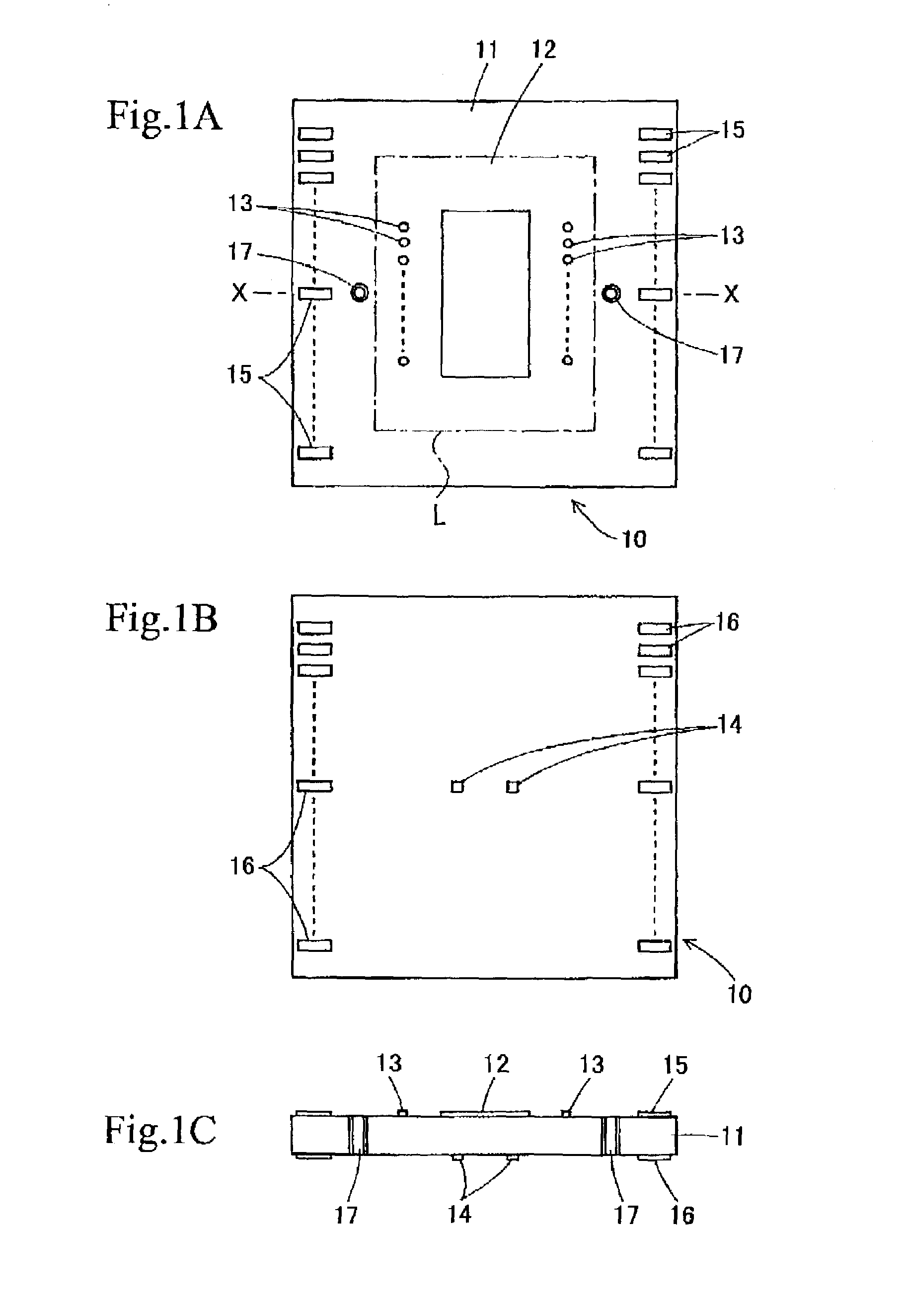
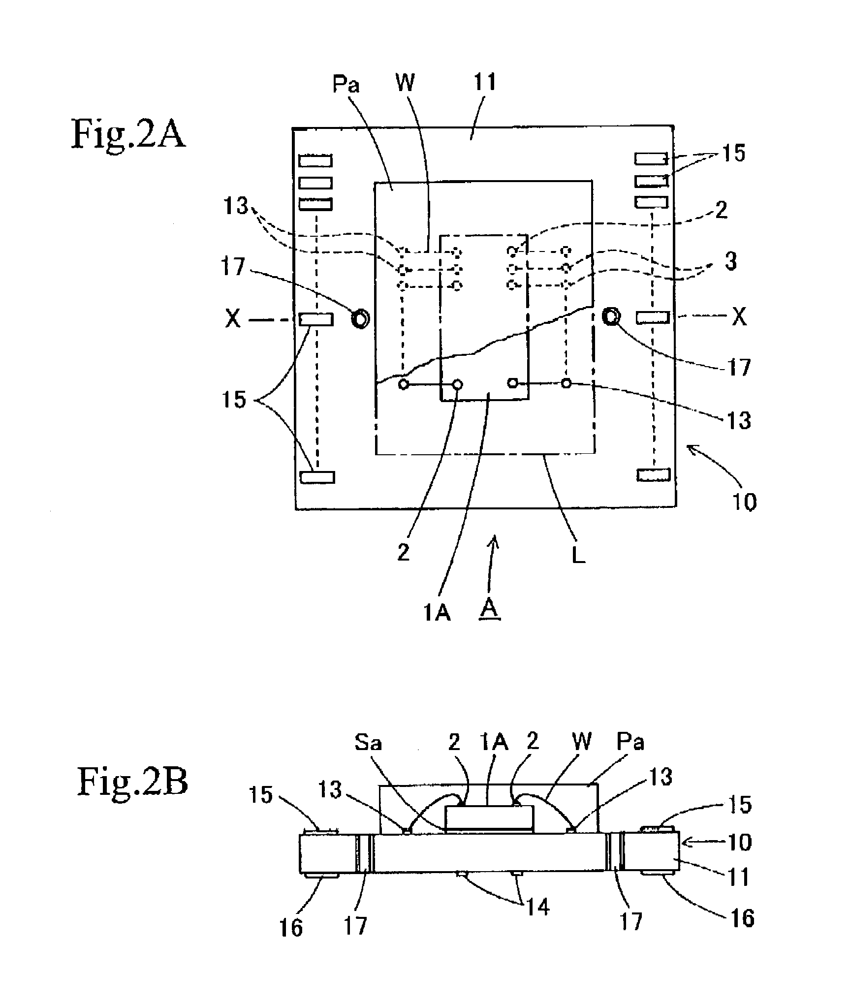
[0041]Next, by use of FIGS. 2A and 2B, the structure of a semiconductor device according to the present invention will be described.

[0042]In FIGS. 2A and 2B, symbol A denotes the semiconductor device according to the first embodiment of the present invention. The semiconductor device A is comprised of an IC chip 1A (the same as the IC chip 1) and a printed wiring board 10, in the same manner as the semiconductor device C according to the related art. On the surface of the IC chip 1A, a plurality of bumps 2 of gold, solder or the like are provided on the surfaces of electrodes provided in a predetermined arrangement.

[0043]The IC chip 1A is adhered and fixed to the mount portion 12 of the printed wiring board 10 shown in FIG. 1A, for example, through a conductive adhesive Sa. The individual bumps 2 are electrically connected to the corresponding lands 13 respectively by metallic thin wires W of gold or the like. The semiconductor device A also is constituted in a structure in which th...

second embodiment

[0044]A semiconductor device B according to the present invention shown in FIG. 3 has a structure in which a printed wiring board 10 having the above-mentioned structure is used, an IC chip 1B smaller in thickness than the IC chip 1A is mounted on a central portion of the printed wiring board 10, and the IC chip 1B inclusive of connection portions between bumps 2 and lands 13 is sealed with a sealing material Pb smaller in thickness than the printed wiring board 10.

[0045]In the semiconductor device A and the semiconductor device B thus provided with the external connection electrodes 15 and 16, the external connection electrodes 15 and 16 are provided at outer peripheral portions of the printed wiring board 10, as contrasted to the semiconductor device C according to the related art in which the external connection electrodes 114 are provided on the back side. Therefore, by combining the connections of these external connection electrodes 15 and 16, it is possible to obtain a semico...

fourth embodiment

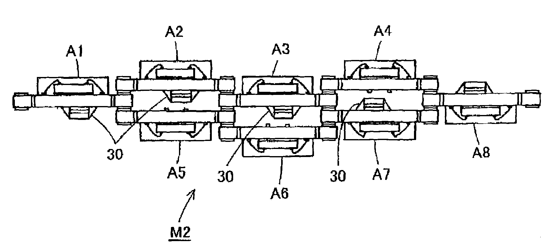
[0053]FIG. 7 shows the semiconductor module M4 according to the present invention. The semiconductor module M4 is constituted of three semiconductor devices B. The semiconductor module M4 has a structure that is preferable where a semiconductor module with a small overall thickness is desired. Namely, the semiconductor devices B1 and B3 are mounted on a mount base (not shown) such as a jig at a predetermined interval, the semiconductor device B2 to be mounted later is inverted face side back, and they are connected by the same soldering method as described above. When the semiconductor module is constituted in such a structure, a semiconductor module having a roughly uniform thickness on the whole is obtained.


PUM


Abstract

The present invention is directed to a semiconductor device and a semiconductor module both having an inexpensive and compact structure. The semiconductor module (M1) according to a first embodiment of the present invention is comprised of a plurality of semiconductor devices (A1) through (A3) having a structure that includes external connection electrodes (15) and (16) being provided on both the face side and the back side of outer peripheral portions of a printed wiring board (10), and a semiconductor integrated circuit chip (1A) being mounted on a central portion of the printed wiring board (10). The external connection electrodes (15) of the semiconductor devices (A1) and (A3) and the external connection electrodes (16) of the semiconductor device (A2) are electrically connected to each other by solder Sb, for example, either directly or through a chip part (30) or a relay board (40).

Description

TECHNICAL FIELD[0001]The present invention relates to the structures and constitutions of a semiconductor device and a semiconductor module in which a plurality of semiconductor devices are incorporated.BACKGROUND ART[0002]First, referring to FIGS. 10 to 13, the constitutions and structures of a semiconductor device and a semiconductor module according to the related art will be described.[0003]FIG. 10 is a sectional view of a semiconductor device according to one embodiment of the related art, FIG. 11 is a sectional view of the structure in which the semiconductor device shown in FIG. 10 is mounted on a mother board, FIG. 12 is a sectional view of a semiconductor module in which a plurality of semiconductor devices shown in FIG. 10 are mounted on a mother board, and FIG. 13 is a sectional view of a semiconductor module according to another embodiment in which a plurality of semiconductor devices shown in FIG. 10 are mounted on a mother board.[0004]First, the constitution and struct...

Claims


Application Information

Patent Timeline
IPC IPC(8): H01L23/48H01L23/34H01L25/10H01L25/18H05K1/02H05K1/14H05K1/18
CPCH01L24/73H01L25/105H01L2224/32225H01L2224/48091H01L2224/48227H01L2224/49175H01L2224/73265H01L2225/1005H01L2225/1023H01L2225/1058H01L2225/107H01L2924/01079H01L2924/14H01L2924/1433H01L2924/15311H01L2924/15321H01L2924/181H01L2924/19041H01L2924/19106H05K1/0231H05K1/141H05K1/182H01L2924/00014H01L2924/00H01L2924/00012H01L23/48
Inventor FUKASAWA, HIROYUKI
Owner SONY CORP
Why Eureka
Try Eureka