Plasma display panel including partition wall member

a plasma display panel and partition wall technology, applied in the direction of gas discharge vessels/containers, gas-filled discharge tubes, electrodes, etc., can solve the problems of increasing costs, affecting the quality of plasma display panels, and requiring compatibility between plasma discharges, so as to reduce manufacturing costs, prevent emissions, and simplify the manufacturing process

Inactive Publication Date: 2006-01-31
PIONEER CORP
View PDF10 Cites 6 Cited by
  • Summary
  • Abstract
  • Description
  • Claims
  • Application Information

AI Technical Summary

Benefits of technology

[0032]With the foregoing plasma display panel, because the row electrode pairs and the column electrodes are formed on one of the pair of substrates facing each other with the discharge space in between, it is possible to simplify the manufacturing process to substantially reduce the manufacturing costs.
[0033]Because the reset discharge and the addressing discharge are caused in the second discharge area which is formed independently of the first discharge area which is provided for producing the sustain discharge for light emission for the generation of the image, it is possible to employ a configuration capable of preventing the emissions caused by the reset discharge and the addressing discharge from leaking toward the display screen of the panel for the prevention of a reduction in the dark-light contrast of the image.
[0034]Further, there is no need to provide a phosphor layer in the second discharge area in which the addressing discharge is produced. This makes it possible to avoid the effects of the phosphor layer on: the discharge characteristics varying among the individual phosphor materials of the colors of the phosphor layers; a change in discharge voltage caused by the phosphor layer, for example, caused by variations in the thickness of the phosphor layer occurring when the phosphor layer is formed in the manufacturing process; and the like. This ensures the uniformity of the addressing discharge characteristics in each second discharge area, to improve a margin in the addressing discharge.
[0035]Still further, the first discharge area is only required to produce the sustain discharge. For this reason, the limitations imposed on the structure of the first discharge area are decreased, resulting in the possibility of optimizing the structure of the first discharge area for the sustain discharge.

Problems solved by technology

Therefore, this conventional PDP has the problem of the entailing high manufacturing costs and a further increase in costs due to the large number of components formed on each substrate.
When the cell structure is designed, the necessity for compatibility between those discharges gives rise to considerable restrictions.
This involves the problem of difficulties arising in providing the adequate discharge characteristics in any discharge.
For this reason, the conventional PDP has the problem of significant difficulties arising in providing equal addressing discharge characteristics in all the discharge cells C.

Method used


Image

  • Plasma display panel including partition wall member
  • Plasma display panel including partition wall member
  • Plasma display panel including partition wall member

Examples


first embodiment

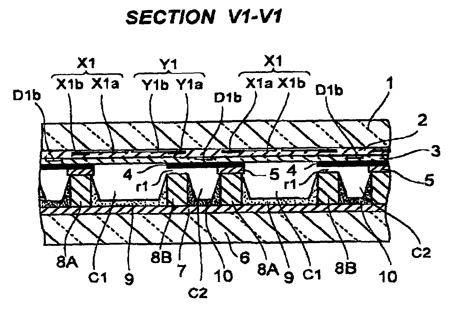
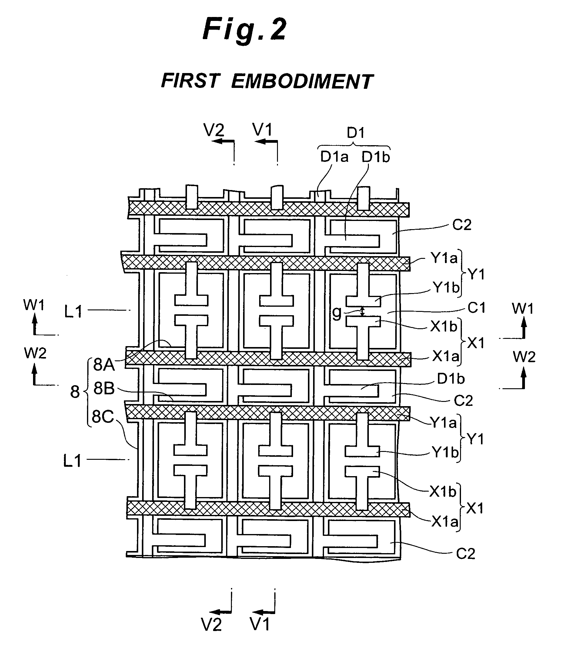
[0054]FIG. 2 to FIG. 6 are diagrams illustrating a plasma display panel (hereinafter referred to as “PDP”) according to the present invention: FIG. 2 is a schematic front view of the PDP and FIGS. 3, 4, 5 and 6 are sectional views respectively taken along the V1—V1 line, the V2—V2 line, the W1—W1 line and the W2—W2 line as shown in FIG. 2.

[0055]In FIG. 2 to FIG. 6, a plurality of row electrode pairs (X1, Y1) each extending in the row direction of a front glass substrate 1 (i.e. the right-left direction in FIG. 2) are arranged parallel to each other on the rear-facing face of the front glass substrate 1 serving as the display screen.

[0056]The row electrode X1 is composed of a black- or dark-colored bus electrode X1a formed of a metal film extending in the row direction of the front glass substrate 1, and T-shaped transparent electrodes X1b formed of a transparent conductive film made of ITO or the like. The transparent electrodes X1b are lined up along the bus electrode X1a at regula...

second embodiment

[0093]FIG. 7 to FIG. 11 are diagrams illustrating the PDP according to the present invention: FIG. 7 is a schematic front view of the PDP and FIGS. 8, 9, 10 and 11 are sectional views respectively taken along the V3—V3 line, the V4—V4 line, the W3—W3 line and the W4—W4 line as shown in FIG. 7.

[0094]In FIG. 7 to FIG. 11, a plurality of row electrode pairs (X2, Y2) each extending in the row direction of a front glass substrate 1 (i.e. the right-left direction in FIG. 7) are arranged parallel to each other on the rear-facing face of the front glass substrate 1 serving as the display screen.

[0095]The row electrode X2 is composed of a bus electrode X2a formed of a black- or dark-colored metal film extending in the row direction of the front glass substrate 1, and T-shaped transparent electrodes X2b formed of a transparent conductive film made of ITO or the like. The transparent electrodes X2b are lined up along the bus electrode X2a at regular intervals, and connected to the bus electrod...

third embodiment

[0134]FIG. 12 to FIG. 16 are diagrams illustrating the PDP according to the present invention: FIG. 12 is a schematic front view of the PDP and FIGS. 13, 14, 15 and 16 are sectional views respectively taken along the V5—V5 line, the V6—V6 line, the W5—W5 line and the W6—W6 line as shown in FIG. 12.

[0135]In FIG. 12 to FIG. 16, row electrodes X3 and row electrodes Y3 each extending in the row direction of a front glass substrate 1 (i.e. the right-left direction in FIG. 12) are regularly arranged in alternate positions at required intervals in the column direction on the rear-facing face of the front glass substrate 1 serving as the display screen.

[0136]The row electrode X3 is composed of a bus electrode X3a formed of a black- or dark-colored metal film extending in the row direction of the front glass substrate 1, and transparent electrodes X3b formed of a transparent conductive film made of ITO or the like. The transparent electrodes X3b are lined up along the bus electrode X3a at re...


PUM


Abstract

In the PDP, a discharge cell is formed in the vicinity of an intersection of a row electrode pair and a column electrode. The column electrode is formed in a different plane within a dielectric layer from that in which the row electrode pair is formed. Each of the discharge cells is surrounded and defined by a partition wall member, and divided by a second transverse wall into a display discharge cell for producing a sustain discharge and an addressing discharge cell for producing a reset discharge and an addressing discharge. The display discharge cell and the addressing discharge cell communicate by means of a clearance.

Description

BACKGROUND OF THE INVENTION[0001]1. Field of the Invention[0002]This invention relates to a panel structure for surface-discharge-type AC plasma display panels.[0003]The present application claims priority from Japanese Application No. 2003-137270, the disclosure of which is incorporated herein by reference.[0004]2. Description of the Related Art[0005]Surface-discharge-type AC plasma display panels (hereinafter referred to as “PDP”) have recently gained the spotlight as types of large-sized slim color display apparatuses and are becoming increasingly common in homes and the like.[0006]Such known surface-discharge-type AC PDP includes a three-electrode reflection-type PDP.[0007]The structure of the three-electrode reflection-type PDP is described here. The front glass substrate is placed opposite the back glass substrate with a discharge-gas-filled discharge space in between. On the inner surface of the front glass substrate, a plurality of row electrode pairs and a dielectric layer ...

Claims


Application Information

Patent Timeline
Patent Type & Authority Patents(United States)
IPC IPC(8): H01J17/49H01J11/14H01J11/22H01J11/24H01J11/26H01J11/32H01J11/34H01J11/36H01J11/38H01J11/44
CPCH01J11/12H01J11/24H01J11/32H01J2211/323H01J2211/245
Inventor HASHIKAWA, HIROKAZUTOGASHI, TAKAHIRO
Owner PIONEER CORP
Why Eureka
Try Eureka