Solid state vacuum devices and method for making the same

a solid-state semiconductor and vacuum device technology, applied in the direction of discharge tube main electrodes, discharge tube luminescnet screens, tubes with electrostatic control, etc., can solve the problems of inter-electrode electron leakage, high frequency or severe environmental conditions, and vacuum tube remaining in use,

Inactive Publication Date: 2006-02-07
INNOSYS
View PDF48 Cites 9 Cited by
  • Summary
  • Abstract
  • Description
  • Claims
  • Application Information

AI Technical Summary

Benefits of technology

[0007]In one specific embodiment, the present invention provides an SSVD in a diode configuration. In this embodiment, the SSVD comprises a substrate having a cavity formed into the substrate. The SSVD further comprises a cathode in the form of an air bridge suspended over the cavity of the sub

Problems solved by technology

The result is that today more circuits are utilizing solid-state semiconductor devices, with vacuum tubes remaining in use only in limited circumstances such as those involving high power, high frequency, or hazardous environmental applications.
In these limited circumstances,

Method used


Image

  • Solid state vacuum devices and method for making the same
  • Solid state vacuum devices and method for making the same
  • Solid state vacuum devices and method for making the same

Examples


Embodiment Construction

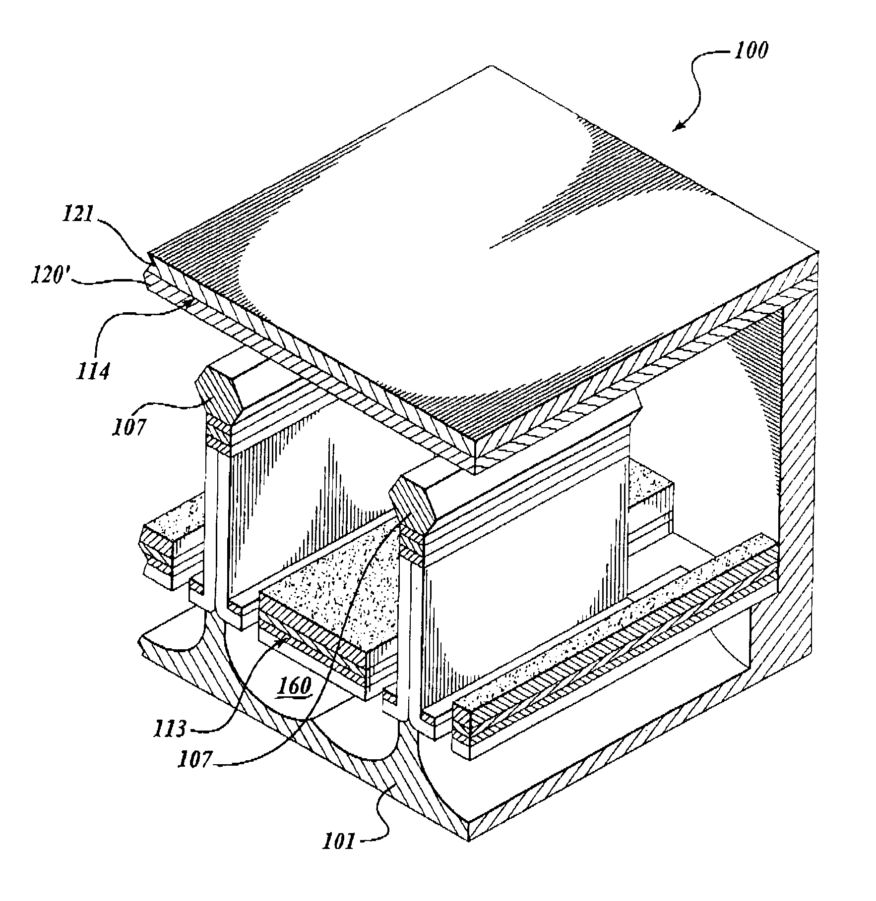
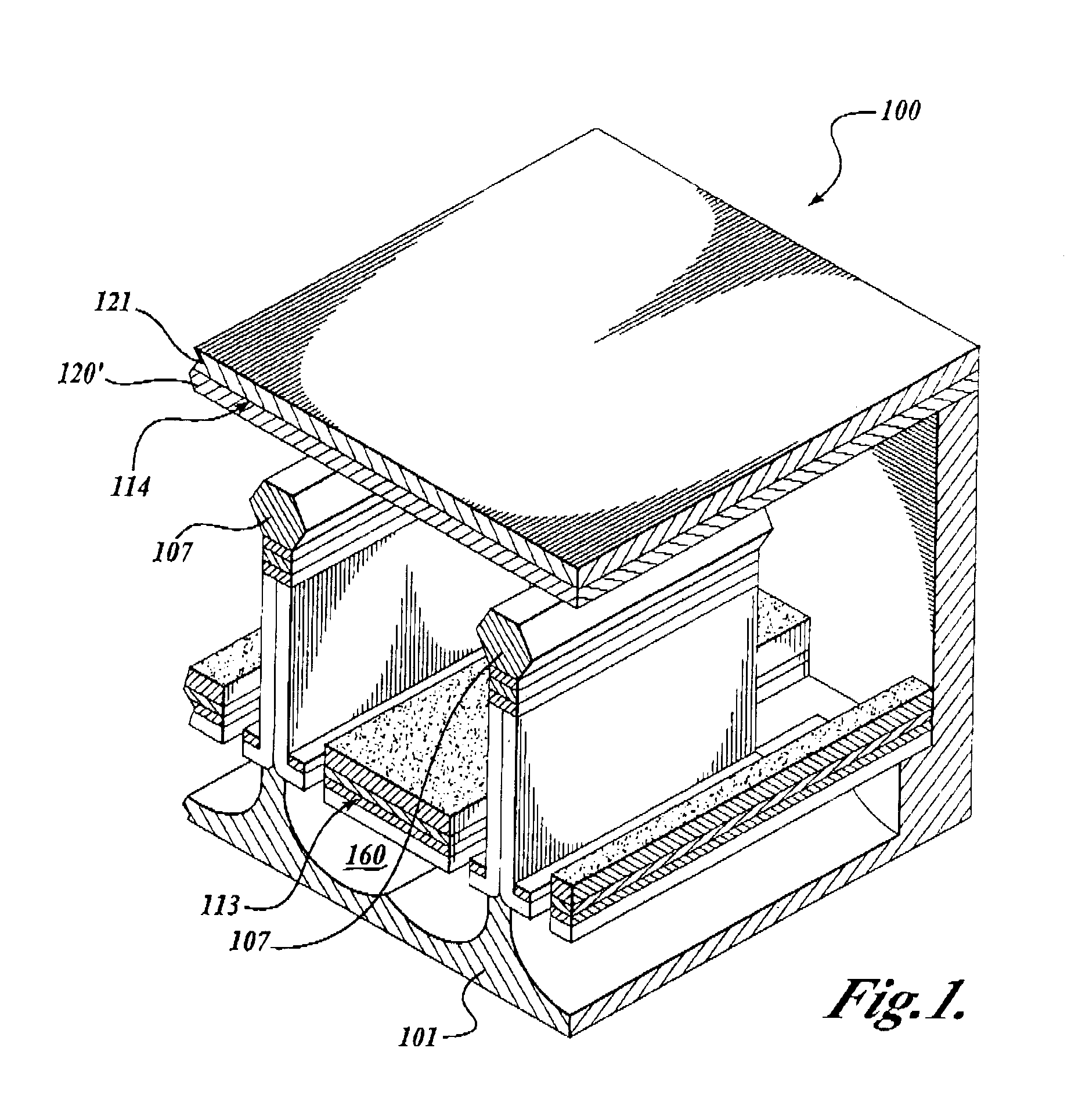
[0022]The present invention provides a sub micron-scale to cm-scale and beyond, solid-state vacuum device that operates in a manner similar to that of a traditional vacuum tube devices. As described below, the present invention includes a plurality of embodiments where a device is configured to form a diode, triode, tetrode, pentode or other higher order devices made from novel semiconductor fabrication techniques. The following sections provide a detailed description of each embodiment and several fabrication methods for making the devices disclosed herein. Supplemental information is also provided in a contemporaneously filed patent application entitled “Solid State Vacuum Devices and Method for Making the Same,” which is commonly assigned to InnoSys, Inc. of Salt Lake City, Utah, and naming Ruey-Jen Hwu and Larry Sadwick as co-inventors; the subject matter of which is incorporated by reference.

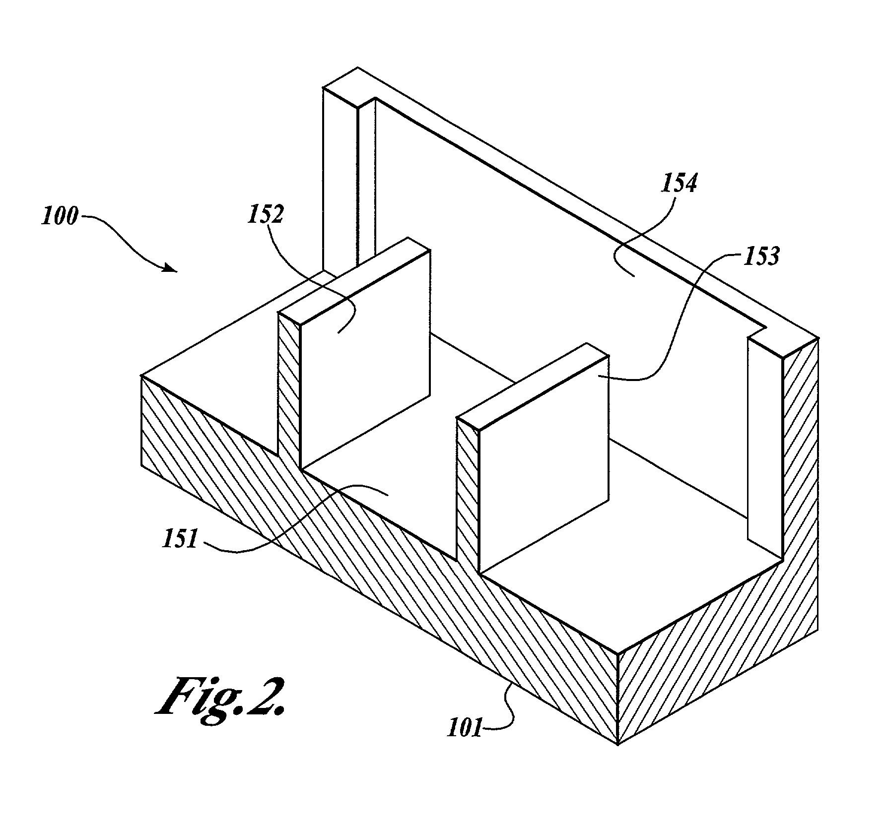
[0023]Referring now to FIG. 1, the basic elements of one embodiment of a triode solid s...


PUM


Abstract

A solid-state vacuum device (SSVD) and method for making the same. In one embodiment, the SSVD forms a triode device comprising a substrate having a cavity formed therein. The SSVD further comprises cathode positioned near the opening of the cavity, wherein the cathode spans over the cavity in the form of a bridge that creates an air gap between the cathode and substrate. In addition, the SSVD further comprises an anode and a grid that is positioned between the anode and cathode. Upon applying heat to the cathode, electrons are released from the cathode, passed through the grid, and received by the anode. In response to receiving the electrons, the anode produces a current. The current received by the anode is controlled by a voltage applied to the grid. Other embodiments of the present invention provide diode, tetrode, pentode, and other higher order device configurations.

Description

FIELD OF THE INVENTION[0001]The present invention relates to semiconductor devices and vacuum devices, and in particular, to devices configured to operate in a vacuum environment and devices manufactured through microelectronic, micro electro-mechanical systems (MEMS), micro system technology (MST), micromachining, and semiconductor manufacturing processes.BACKGROUND OF THE INVENTION[0002]Vacuum tubes were developed at or around the turn of the century and immediately became widely used for electrical amplification, rectification, oscillation, modulation, and wave shaping in radio, television, radar, and in all types of electrical circuits. With the advent of the transistor in the 1940s and 1950s and integrated circuit technology in the 1960s, the use of the vacuum tube began to decline, as circuits previously employing vacuum tubes were adapted to utilize solid-state transistors. The result is that today more circuits are utilizing solid-state semiconductor devices, with vacuum tub...

Claims


Application Information

Patent Timeline
IPC IPC(8): H01J1/46H01J1/13H01J1/62H01J3/02H01J21/10
CPCH01J1/13H01J1/46H01J21/105H01J19/38H01J3/027
Inventor HWU, RUEY-JENSADWICK, LARRY
Owner INNOSYS
Why Eureka
Try Eureka