Method of adjusting CoFe free layer magnetostriction
a free layer and magnetostriction technology, applied in the direction of magnets, solid-state diffusion coatings, instruments, etc., can solve the problem of reducing the output of the head, and achieve the effect of low coercivity and low positive magnetostriction constan
- Summary
- Abstract
- Description
- Claims
- Application Information
AI Technical Summary
Benefits of technology
Problems solved by technology
Method used
Image
Examples
1st embodiment
1st Embodiment
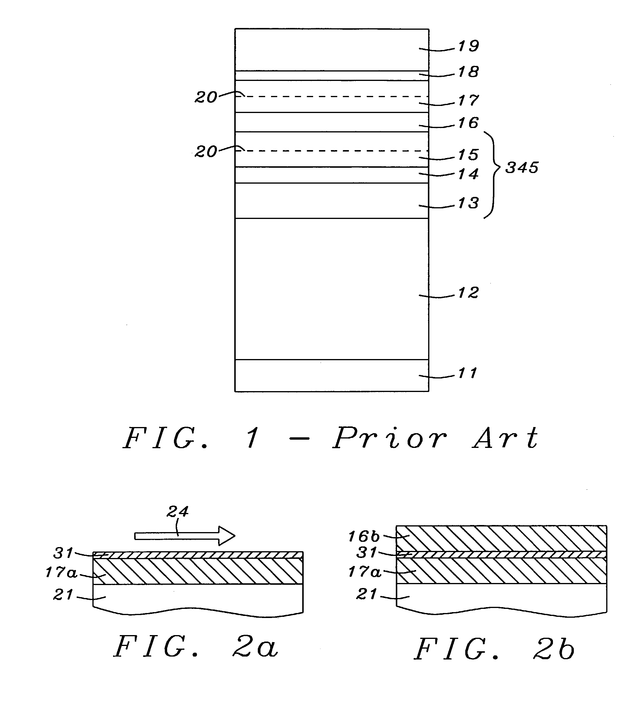
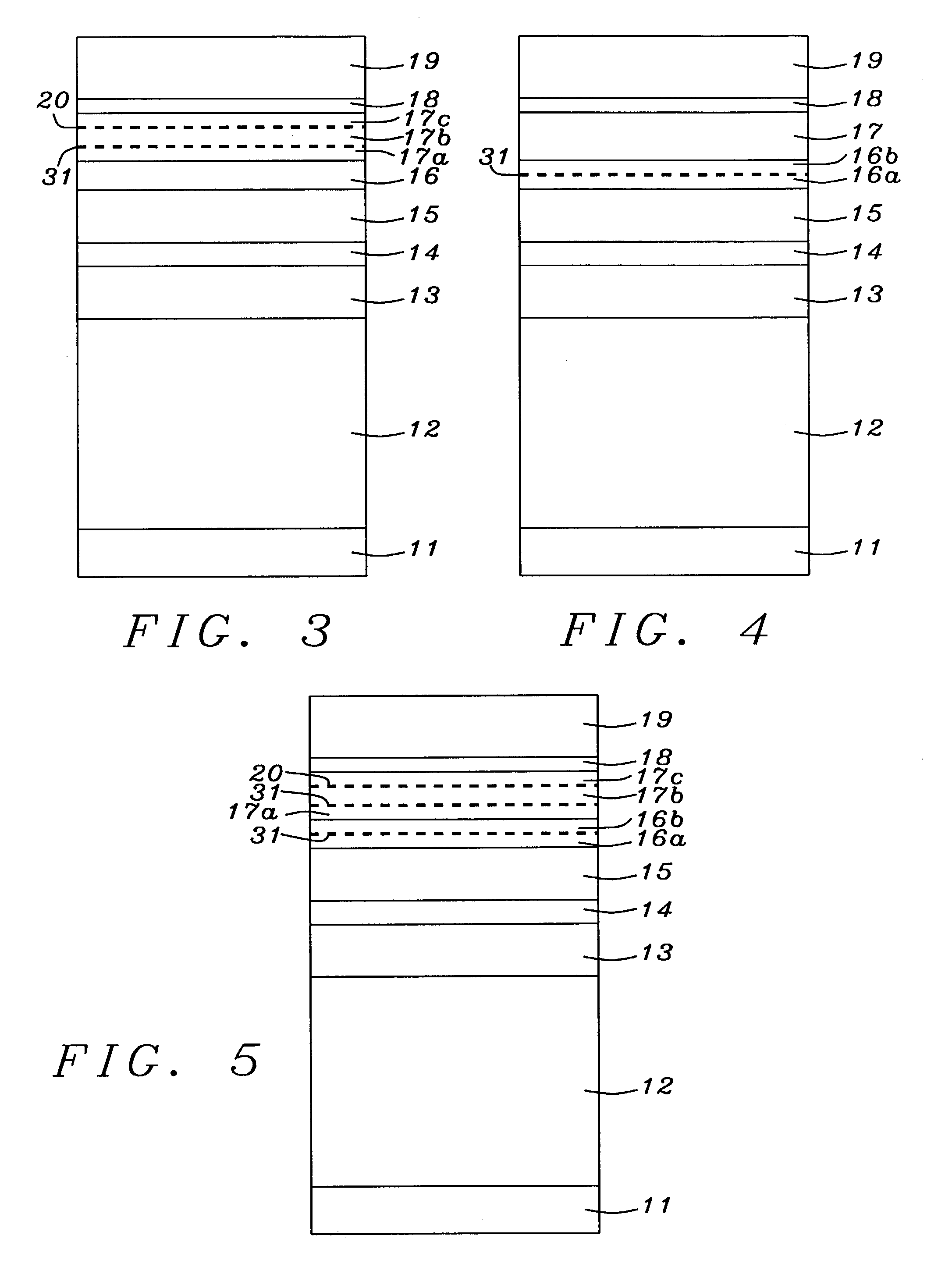
[0030]Referring now to FIG. 5, the process of the present invention begins with the provision of a substrate (not shown) on which is deposited seed layer 11. Typical materials for the latter include NiCr and Ta. The purpose of the seed layer is to provide an improved nucleating surface for antiferromagnetic layer 12 which is deposited next and which will serve as a pinning layer. Layer 12 can be MnPt, IrMn, NiMn, or similar material. The synthetic antiferromagnet, made up of layers 13, 14, and 15 (which was discussed earlier) is now deposited and becomes the pinned layer.
[0031]Following deposition of the pinned layer, in a departure from the prior art, copper sub-layer 16a is deposited to a thickness between about 5 and 20 Angstroms, less then the full thickness of the spacer. Layer 16a is then exposed to oxygen in the manner already described above so that its surface becomes equivalent to layer 31 seen earlier as part of the free layer.
[0032]This is followed by the d...
2nd embodiment
2nd Embodiment
[0038]Referring now to FIG. 3, the process for this embodiment begins with the provision of a substrate (not shown) on which is deposited seed layer 11. Typical materials for the latter include NiCr and Ta. The purpose of the seed layer is to provide an improved nucleating surface for antiferromagnetic layer 12 which is deposited next and which will serve as a pinning layer. Layer 12 can be MnPt, IrMn, NiMn, or similar material. The synthetic antiferromagnet, made up of layers 13, 14, and 15 (which was discussed earlier) is now deposited and becomes the pinned layer. This is followed by the deposition of copper spacer layer 16.
[0039]Next, in a departure from prior art practice, the CoFe free layer is deposited in three stages. The first of these is sub-layer 17a which is deposited onto copper spacer layer 16 to a thickness between about 5 and 15 Angstroms. Then, copper sub-layer 31 is deposited on CoFe sub-layer 17a.The thickness of layer 31 (and other copper sub-layer...
3rd embodiment
3rd Embodiment
[0044]As seen in FIG. 4, this embodiment is similar to the second embodiment for all steps up to completion of the pinned layer. Formation of the spacer layer is, however, different from the prior art:
[0045]Following deposition of the pinned layer, copper sub-layer 16a is deposited to a thickness between about 5 and 20 Angstroms, less then the full thickness of the spacer. Layer 16a is then exposed to oxygen in the manner already described above so that its surface becomes equivalent to layer 31 seen earlier as part of the free layer.
[0046]This is followed by the deposition of second copper sub-layer 16b on sub-layer 31 to complete formation of the spacer layer to a total thickness between about 6 and 21 Angstroms. The remainder of the process of the second embodiment follows standard sub-processes—deposition of contacting layer 18 and cap layer 19.
PUM
| Property | Measurement | Unit |
|---|---|---|
| thickness | aaaaa | aaaaa |
| thickness | aaaaa | aaaaa |
| thickness | aaaaa | aaaaa |
Abstract
Description
Claims
Application Information

