Supercharge Your Innovation With Domain-Expert AI Agents!

Method of manufacturing liquid crystal display device

a liquid crystal display and manufacturing method technology, applied in the direction of optics, instruments, electrical equipment, etc., can solve the problems of increasing the manufacturing cost of more equipment, reducing and reducing the time for attaching the polarizing plate to the liquid crystal display unit cell. , to achieve the effect of enhancing the productivity of manufacturing the liquid crystal display device and reducing the time for attaching the polarizing pla

Inactive Publication Date: 2006-02-14
SAMSUNG DISPLAY CO LTD
View PDF8 Cites 14 Cited by
  • Summary
  • Abstract
  • Description
  • Claims
  • Application Information

AI Technical Summary

Benefits of technology

The present invention provides a method for manufacturing a liquid crystal display device with improved productivity and reduced manufacturing time. The method involves forming thin film transistor and color filter unit cells on separate mother substrates, aligning them to face each other, and then assembling them to form an assembled substrate. A liquid crystal alignment film is applied to the assembled substrate to facilitate the alignment of liquid crystal molecules. The assembled substrate is then inspected for defects, and a polarizing plate is attached onto the substrate if it passes inspection. The liquid crystal display unit cells are then separated from the assembled substrate, reducing the time for attaching the polarizing plate and increasing productivity.

Problems solved by technology

However, the conventional manufacturing processes has some critical problems.
However, the more equipment greatly increases manufacturing cost.
Further, the conventional manufacturing processes have many problems.
A first problem occurs in the rubbing process.
The particles may induce failures during the rubbing process.
Therefore, the conventional rubbing process cannot be successively performed and the efficiency of manufacturing the liquid crystal display device is lowered.
Therefore, defects of the alignment grooves are seldom detected, when the alignment grooves are already formed.
The defects of the alignment grooves may be detected in the reliability test of the liquid crystal display device after the liquid crystal display device is completely manufactured.
The liquid crystal display device having a defect of the alignment groove lowers image display quality.
A second problem occurs after the assembled substrate is manufactured.
A fourth problem occurs in the module process.
Therefore, much time is required so as to attach the polarizing plate onto the assembled substrate.
However, it is hard to detect the defect of the liquid crystal display device unit cell before cutting off the assembled substrate.
When a polarizing plate is attached onto a defective liquid crystal display unit cell, the polarizing plate is wasted.

Method used


Image

  • Method of manufacturing liquid crystal display device
  • Method of manufacturing liquid crystal display device
  • Method of manufacturing liquid crystal display device

Examples


Embodiment Construction

[0074]Hereinafter the preferred embodiment of the present invention will be described in detail with reference to the accompanying drawings.

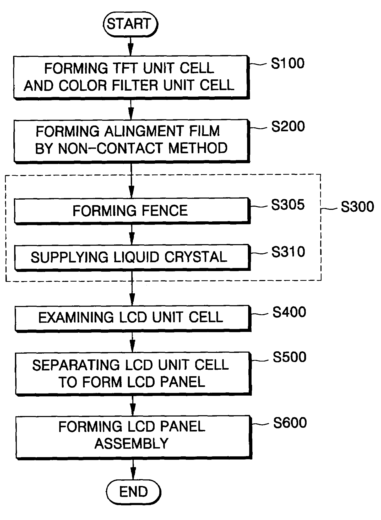
[0075]FIG. 1 is a flow chart showing a method of manufacturing a liquid crystal display device according to a first exemplary embodiment.

[0076]Referring to FIG. 1, at least one thin film transistor unit cell is formed on a first mother substrate, and at least one color filter unit cell is formed on a second mother substrate (step S100). The thin film transistor unit cell formed on the first mother substrate and the color filter unit cell formed on the second mother substrate are formed via different process from each other.

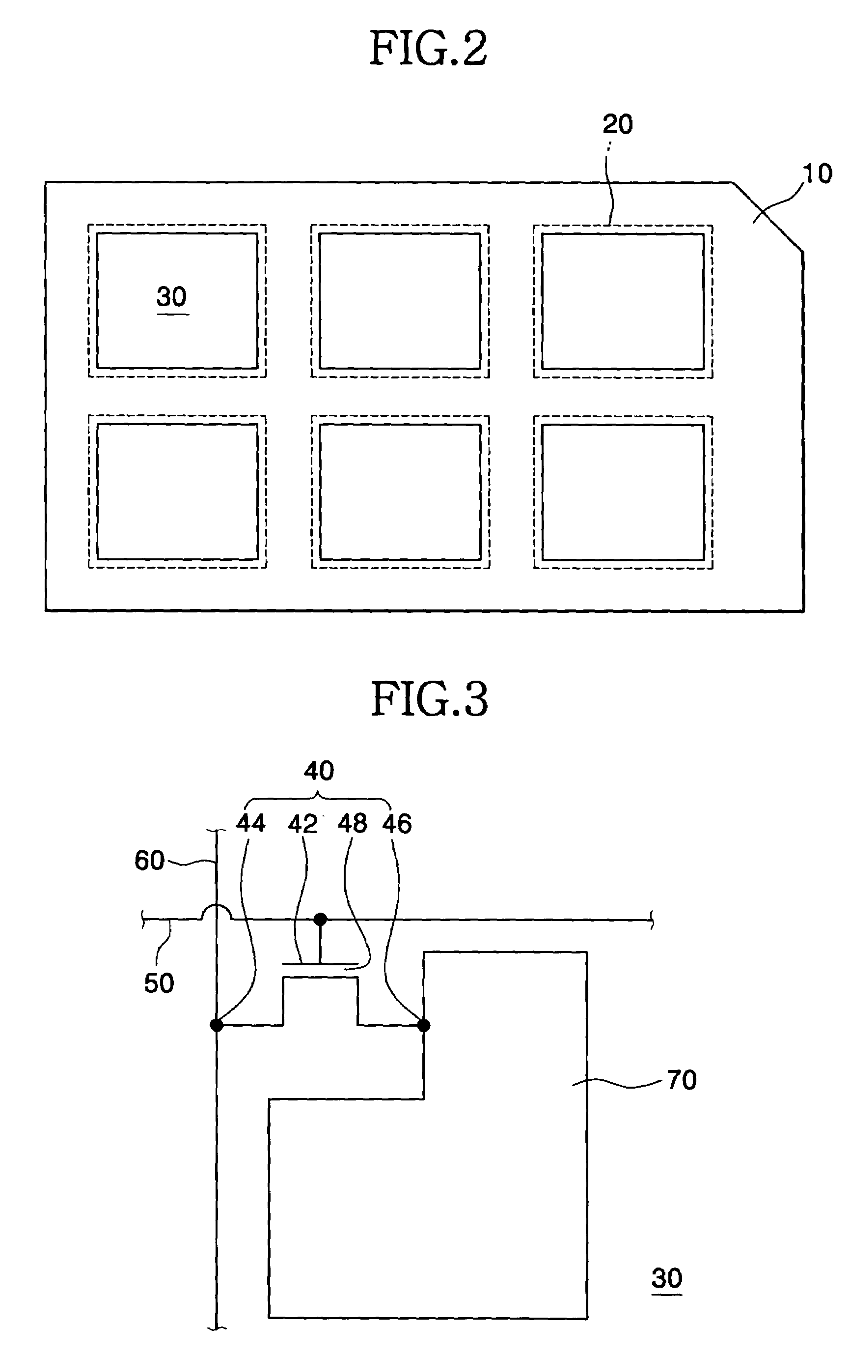
[0077]FIG. 2 is a schematic view showing a first mother substrate and thin film transistor unit cell regions formed on the first mother substrate according to the first exemplary embodiment.

[0078]Referring to FIG. 2, at least one thin film transistor unit cell regions 20 is formed on the first mother substrate 10.

[0079]For exa...


PUM

PropertyMeasurementUnit
angleaaaaaaaaaa
sizeaaaaaaaaaa
temperatureaaaaaaaaaa

Abstract

In a method of manufacturing an LCD device, TFT unit cells are formed on a first mother substrate, and color filter unit cells are formed on a second mother substrate. A liquid crystal alignment film is formed on the TFT unit cells and on the color filter unit cells. The first mother substrate and the second mother substrate are assembled to form an assembled substrate and liquid crystal is disposed between the TFT unit cell and the color filter unit cell. An LCD unit cell is inspected by applying a test driving signal via non-contact method. The LCD unit cell is separated from the assembled substrate to form an LCD panel. A driving module and the LCD panel are assembled to be formed an LCD assembly.

Description

CROSS-REFERENCE TO RELATED APPLICATIONS[0001]This application relies for priority upon Korean Patent Application No.2002-72796 filed on Nov. 21, 2002, the contents of which are herein incorporated by reference in its entirety.BACKGROUND OF THE INVENTION[0002]1. Field of the Invention[0003]The present invention relates to a method of manufacturing a liquid crystal display device, and more particularly to a method of manufacturing a liquid crystal display device having a reduced time for manufacturing the liquid crystal display device and an enhanced productivity.[0004]2. Description of the Related Art[0005]In general, a liquid crystal display device is lighter and smaller in comparison with other display devices. The liquid crystal display devices are manufactured via many manufacturing processes.[0006]A first process for manufacturing the liquid crystal display device includes forming thin film transistor (tft) unit cells on a first mother substrate and forming color filter unit cel...

Claims


Application Information

Patent Timeline
Patent Type & Authority Patents(United States)
IPC IPC(8): G02F1/13G02F1/133G02F1/1347G02F1/1337G02F1/1341
CPCG02F1/1309G02F1/1337G02F1/1341G02F1/133711G02F2001/13415G02F1/13415G02F1/13
Inventor CHOO, DAE-HOCHOI, DONG-UKCHO, SANG-KYU
Owner SAMSUNG DISPLAY CO LTD
Features
  • R&D
  • Intellectual Property
  • Life Sciences
  • Materials
  • Tech Scout
  • Unparalleled Data Quality
  • Higher Quality Content
  • 60% Fewer Hallucinations
Learn More